Hi, guys,
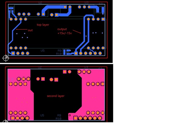
I got a question about the PCB layout of the isolation amplifier ISO121, I place ISO121 on PCB top layer, can I route traces on top layer under ISO121? Thanks !
This thread has been locked.
If you have a related question, please click the "Ask a related question" button in the top right corner. The newly created question will be automatically linked to this question.
Hi, guys,
I got a question about the PCB layout of the isolation amplifier ISO121, I place ISO121 on PCB top layer, can I route traces on top layer under ISO121? Thanks !
Hi Jesse,
It is not recommend to route under the ISO121 as it will reduce the creepage measurement - potentially allowing for arcing depending on the isolation requirements.
If this is not a concern, routing under the device should be fine.
Alexander, thanks for your reply, I just route the output +15v/-15v traces under the device at the output side, is that still have a creepage degradation ? and I put one separated output ground plane on the second layer at output side , and another separated input ground plane on the second layer at the input side, are these ground plane necessary for the device performance ? thanks !

Hi Jesse,
I agree with Kai - U2 and U3 are violating the isolation barrier. I believe you need to reconsider your layout.
U2 is the isolated power supply for ISO121 input side, U3 is the isolated power supply for ISO121 input side. the clearance between the input pins and output pins are more than 3mm, the components also need keep enough body to body clearance ?
Hi Jesse,
Can you provide the schematic?
As the layout is drawn it appears that the isolation barrier is being bypassed by U2 and U3.
Hi Jesse,
What is driving the need for 3 grounds in the system?
We typically recommend a low voltage and a high voltage ground, generating the supply for the high voltage ground via isolated DC/DC converter.
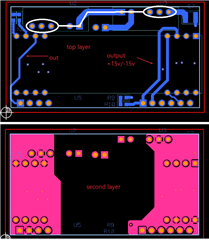
In the current configuration I am concerned of arcing from 0V_IN to 0V_OUT through GND as I've drawn below.

Hi Alexander,
This small board shall be installed to another board to replace ADI AD210, the GND shall be connected to 0V_IN or 0V_OUT depending on the application. the input/output power regulator are also isolated at rated 3000KV. Do you have any suggestion to avoid the arc you mentioned? thanks !
Hi Jesse,
The parts are rated well, it's the layout that is concerning. I would rotate both of the input/output power regulators 90 degrees so that GND is farther away from 0V_IN and 0V_OUT. This of course will increase the size of the board which is non-ideal, however it will reduce the chance of arcing.
Additionally, if this increase in PCB size is not desired, consult the standards for creepage and clearance requirements based on the applied voltage and environmental degree to ensure that the design is within specification.