This thread has been locked.
If you have a related question, please click the "Ask a related question" button in the top right corner. The newly created question will be automatically linked to this question.
Hi Team,
I need help clarifying the inquiry below:
Page 17 mentions the following:
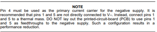
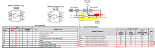
But the layout example shows that pin 1, 4 and 5 is connected
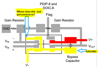
I can connect pin 4 to v- as the main source but it is not clear to me how to connect pins 1 and 5. But it is not clear to me is that pin 5 is connected to the decoupling capacitor pin that goes to ground. Is this correct, and where is the other side of the pin 1 pad connected to?
Looking forward to your response.
Regards,
Marvin
Hi Marvin,
place an isolated, local copper plane or copper fill serving as a heatsink for the OPA551 directly under and arround the OPA551 in the top layer of printed circuit board as symbolized by the yellow copper tracks. Connect this copper plane to the main V- routing only close to pin 4 of OPA551 so that the V- supply current is mainly flowing through pin 4. Connecting V- to only pin 1 and/or pin 5 without connecting pin 4 at all, on the other hand, would violate this rule. Then the supply current would only flow through pin1 and/or pin 5 and would see a too high internal resistance to the die which can make issues. This is meant by "do not use pin1 and pin 5 as feedthrough to V-", since the main connection to V- has to be pin 4.
To improve the situation and to decrease the portion of supply current running through pin 1 and pin 5, connect pin 1 and pin 5 (which are connected to isolated, local copper planes or copper fills) only by rather narrow copper tracks to pin 4, as symbolized by the yellow copper tracks. Or by other words, have local copper planes or copper fills at pins 1, 4 and 5, but connect pin 1 and pin 5 to pin 4 only by rather narrow copper tracks. And connect V- of the board closest to pin 4, so that the main supply current is flowing through pin 4 and -at the same time- pins 1, 4, and 5 can serve as heatsinks.
So, what is connected to the left of pin 1 (and to the right of pin 5) is only an isolated, local copper plane or ground fill serving for cooling. No additional electrical connection should be made there to V- of the board.
Connecting the bypass capacitor to pin 5 instead of pin 4 was correct under the assumption that no relevant current is ever flowing through it, which is wrong of course. So, you are right, I would connect the bypass capacitor to pin 4 and not to pin 5.
Above I talk about "isolated, local copper planes or ground fills". By "isolated" I simply mean isolated from the ground plane or ground fills which are usually laid out on the top layer of printed circuit board
Kai
Hi Marvin,
I would go with Kai's suggestion. This SOIC package does not come with thermal pad, and the SOIC package is using pins1, 4 and 5 for extra heat dissipation. The main V- connection is pin4, as Kai pointed out.
I hope that the designed circuit is operating under a light load. Since I do not have the schematic, I am able to comment on it. If your application is going to draw the full rated current, I would recommend to use KTW package. I can simulate the heat dissipation of your schematic and see if the SOIC package is suitable for the application (you would need to provide the design requirements and schematic).
Based on the Psi resistance figure, the majority of heat is dissipated via the top of the package. If you thermally bond a heat sink on top of the package, then it will likely lower the Tj operating temperature (it depends on how much current is drawn from the IC). You need to tell us more about the application.
Best,
Raymond