This thread has been locked.

If you have a related question, please click the "Ask a related question" button in the top right corner. The newly created question will be automatically linked to this question.

INA851: LTspice model issue

Part Number: INA851
Other Parts Discussed in Thread: TINA-TI

Hello,

I am trying to simulate the behaviour of the INA851 instrumentation amplifier on LTspice using TI model: SBOMC50.ZIP (101 KB) - PSpice Model.

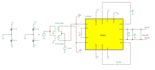
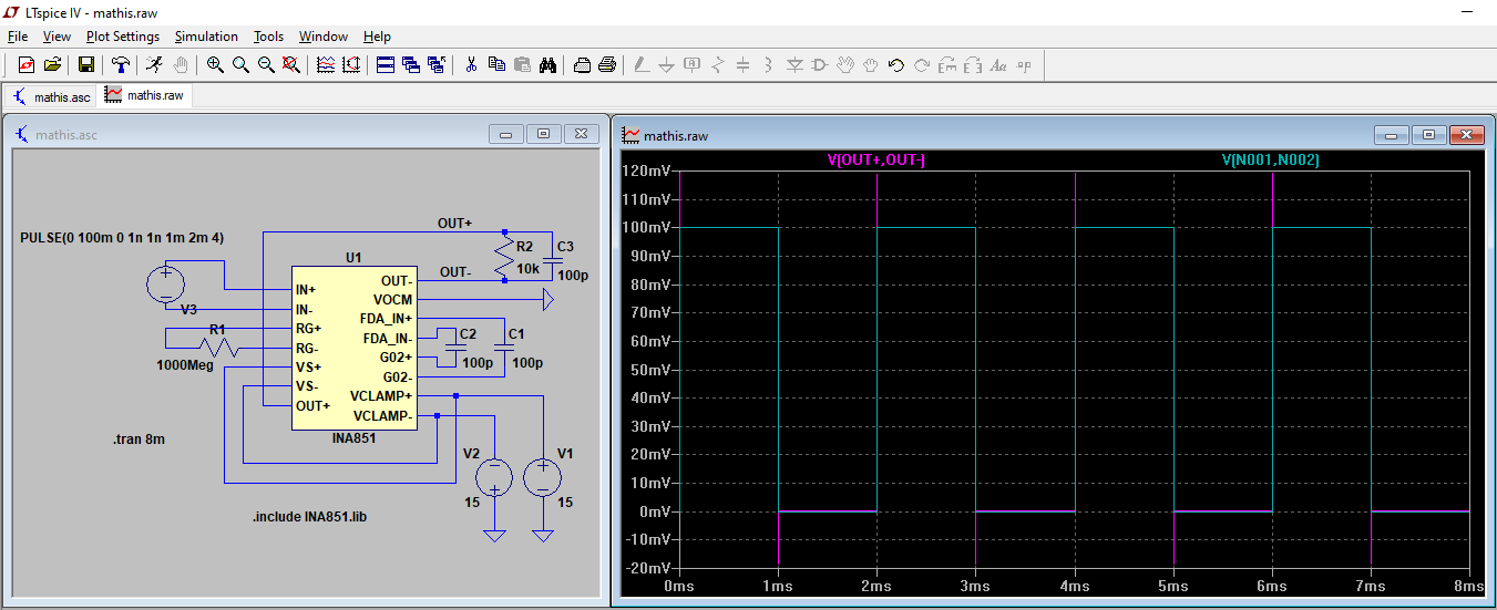
Below is my schematic. The gain is set to 1 (RG open), the output clamping function is not used. The input is a 500Hz/100mV square wave.

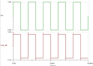
The input/output waveforms are shown below.

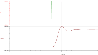
The only good point here is that the output follows the input. However, the dynamics seem very low, the rise and fall times are huge (200us) for a 15MHz bandwidth device. 

Also, the output only follows the input for input amplitudes lower than 500mV. Above, the output saturates at 4V/-4V for some reason.

Does anyone have experienced this before? Any idea what could have gone wrong?

Thank you in advance!

  • Hi Mathis,

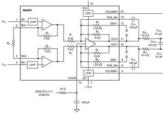
    In the circuit above, there is a 100pF connected between FDA_IN- and FDA_IN+ pins and the G02+ and G02- pins of the fully-differential (FDA) output-stage. For clarification, in general these pins are used to connect capacitors between the FDA_IN- / FDA_IN+ and the OUT+ /OUT- of the device. These CFB capacitors are optional and can be customized to limit bandwidth / filtering the higher frequency noise.  If you require the INA851 full-bandwidth at all gains, you may consider removing the optional capacitors. 

     Nevertheless, when simulating the circuit using TINA-TI simulation tool, with the 100pF G02 - FDA_IN+/- circuit above, I obtain the expected response:

    The INA851 in the configuration above G=1, VOCM+0V, V+/- = ±15V and VCLAMP+/-= ±15V, supports a ±12.5Vp input/output signal.

    Although, on the TINA simulator, I am unable to reproduce the issue with the ±4.5V output limitation described on your post, the clamping function and the input-output range limits on the SPICE model do not simulate properly and this is a known problem on the current model.  I will check with the modeling team regarding the status of the final model correcting the clamping and input-output limits issue.  This issue has been reported to the modeling team, and fixing this issue is in their queue.

    Thank you and Regards,

    Luis

  • Bon soir Mathis,

    works for me in LTspice:

    mathis.zip

    Kai

  • Hi Kai,

    Thank you.

    Hi Mathis,

    We were unable to reproduce the transient issue described on the post above, the INA851 appears to provide the correct transient response. Regarding the clamp and input-output range functionality in the SPICE model, the INA851 is in the queue for a revision; expected to be completed by beginning of June.  

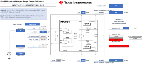
    The INA851 is similar to standard instrumentation amplifiers, the main difference is that incorporates a fully-differential amplifier output.  Each amplifier inside the INA has it’s own input and output swing limitations.   These limitations combine into an overall input differential and common mode voltage versus output swing range limitations as a function of gain, supply voltage, VOCM voltage and Clamp voltage settings. We offer an excel calculator to verify the device is inside the input/output linear range:

    INA851 Input-Output Range Design Calculator

    Attached is a pdf document with instructions:

    INA851 Input and Output Range Design Calculator Instructions.pdf

    Thank you and Best Regards,

    Luis

  • Hi Luis,

    Thank you for your thorough answer. I indeed used the Excel calculator instead, and I stumbled across one small question.

    I will be using only one output (OUT+), referenced to GND. So I need a front-end gain of 2 to obtain an effective gain of 1 between OUT+ and GND. I will use the output clamp between 5V and GND (0V). The negative input is connected to GND. The positive input will see a voltage comprised between -5V and 23V, hence the supply voltage of +25/-10V. And I want to connect VOCM to GND too.

    My question is, with this configuration, why is VOCM highlighted in red in the Excel tool? Actually, the only correct values for VOCM seem to be between 1V and 4V according to this tool. I feel like there is something to do with the clamping function but not sure (?). 

    Thank you a lot in advance for your insight!

    Best regards,

    Mathis

  • HI Mathis,

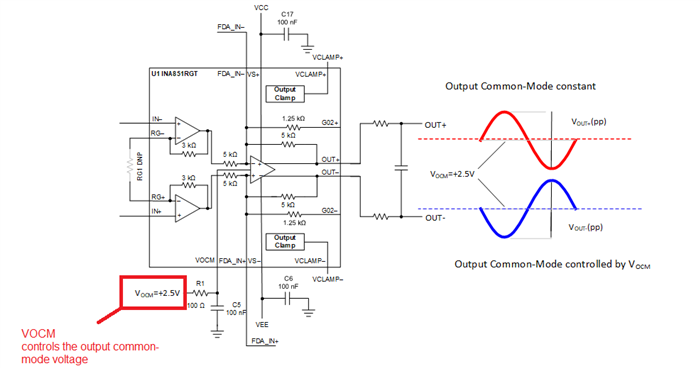
    If the output VCLAMP+ is +5V and VCLAMP- =GND (0V), the VOCM has to be set above GND to provide headroom, somewhere in the middle of your clamp voltage range. In other words, if your output needs to swing between 0 to +5V, the output common-mode needs to be set ideally to VOCM = +2.5V.

    The INA851 is a fully-differential output device, where the device integrates a fully-differential amplifier output stage intended to drive fully-differential circuits, where both OUT- and OUT+ voltages are allowed to swing, centered around the VOCM output common-mode voltage.  The VOCM pin controls the output common-mode voltage.  For example, if VOCM is set to +2.5V, both VOUT- and VOUT+ produce a  fully-differential signal centered at +2.5V:

    Thank you and Regards,

    Luis