Part Number: LM2904
Other Parts Discussed in Thread: LM5026, , LM2903,
Hello:
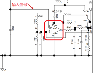
Batch 2221 LM2904DGKR abnormal description: After the main control chip LM5026 of the whole machine detects a fault, the RES output (internal current source current is 7.5-12.5ua) charges the C126 capacitor with a voltage of 2.5V, and pin 3 of IC104 (LM2904DGKR) detects this voltage and compares it with pin 2 (1.17V ) for comparison, and output a high level to the subsequent circuit. When the ambient temperature is 100 ℃, the leakage current of pin 3 is large, so the voltage here cannot rise. Eventually lead to the failure of the functional circuit here. After changing to batch 2144, the input signal level is normal and the circuit works. The partial schematic diagram of the circuit is shown in Figure 1, in which IC104 is the device LM2904DGKR.
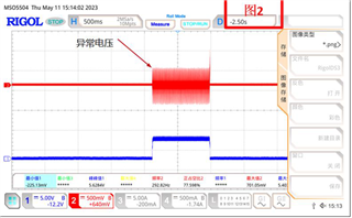
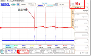
Waveform comparison
Ambient temperature 100℃
CH2 abnormal 2221 batch 3 pin (IN+) to 4 pin (GND) waveform as shown in the figure

The normal 2144 batch 3-pin (IN+) to 4-pin (GND) waveform is shown in the figure

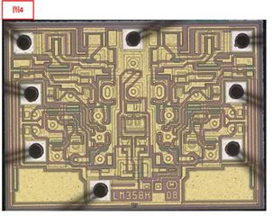
After scanning, the customer found that the silk screen and internal circuit diagrams of the two batches of materials were different.
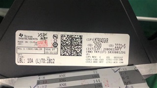
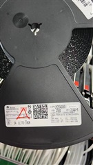
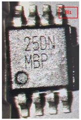
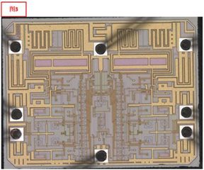
2221 batch silk screen, and DPA diagram, as follows
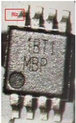
Other batches of 2144 batches of silk screen and DPA pictures are as follows
Please help confirm,Thanks!!!