A related question is a question created from another question. When the related question is created, it will be automatically linked to the original question.
If you have a related question, please click the "Ask a related question" button in the top right corner. The newly created question will be automatically linked to this question.
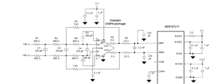
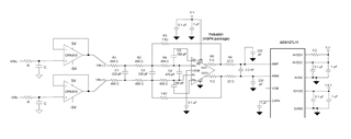
OPA810: power solution for opa810, ths4551 and adc
#1: Though I do not support ADC products outright, I can tell you that 4.5V for AVDD is the exact minimum recommended operating supply voltage for using high-speed mode.
#2: If you power the OPA810 on either +/- 5V or +/-4.5V, the rail to rail input/output will allow enough headroom for a 2.7-4.2V input signal (and the output signal, since the amplifier is in a gain of 1 configuration. Please note the input and output range characteristics in Table 7.5 of the datasheet.
#3: The THS4551 operates on single supply; this device does not have rail to rail inputs. As such, the maximum allowable input voltage on a 5V supply is 3.9V. Your input signal would clip and exceed the maximum allowable input signal on the THS4551. For a 4.5V supply. this value would be even lower. Please refer to Table 7.5, second page, under "Input" of the THS4551 datasheet. The spec notes that the input limitation is Vs+ - 1.1V.
With the current setup, the THS4551 will not be able to handle the full-scale input of the 4.2V input signal coming through the OPA810 circuits. Please examine your input signal requirements and see if you can utilize a lower voltage input signal, or perhaps attenuate the input to the THS4551 slightly. The THS4551 does have rail to rail outputs, which can reach up to 4.8V on a 5V supply.
If you can tighten your input signal range, your two schema are viable. Considering the input limitations of the THS4551, the 5V power solution (solution #1) is preferable.
I do think the first power solution is viable, but it would require a decrease in the input signal level. As you stated, your input signal is 2.7V - 4.2V. A decrease of 0.4V would result in a 2.3V - 3.8V input signal. The voltage peak of 3.8 is below the 3.9 required by a THS4551 on 5V supply. The shift of the lower voltage threshold to 2.3V would not violate any input or output limitations on the negative rail, as Vs- = GND.
I think a small DC offset would be the quickest way to amend the mismatch of input signal to common mode input range. If changing the input signal is not an option, you would need to operate with 0.3V higher supply on the THS4551 for operation at 25C. A 5.3V supply would result in a maximum input voltage of 4.2, which aligns with your signal needs.
Another important point is that the headroom increases if you are operating over -40C to 85C temperature range, in which case the maximum allowable input voltage is 1.2V from the power rail. This would require a 5.4V supply on the THS4551, which is the maximum recommended operating condition. The absolute maximum of the THS4551 is 5.5V.
In summary, you can either raise the supply voltage on the THS4551, or decrease your maximum input signal voltage by DC offset or attenuation.
I understand better now; thank you for being patient with me and my advice. I appreciate your consideration on following the recommended operating conditions for the THS4551.
I did review your power solution; I did not see any issues or areas of concern from my perspective. The typical (TYP) values for quiescent current (Iq) for the THS4551 and OPA810 are 45mA (THS4551) and 3.7mA (x2) for the two channels of the OPA810. This results in the two amplifier solution having a net quiescent current draw of 52.4mA. The OPA810 can output 75mA current, and the THS4551 can drive a maximum of 65mA output. After considering the sum of these currents, and acknowledging a more detailed power consumption analysis could be performed on the entire circuit if needed, the amplifier section can likely draw up to 200mA. As this sequence of OPA810 -> THS4551 -> ADC is repeated for a total of 4 iterations, and the ADC power consumption is not included in my calculations, this sub-circuit can draw around 1A at worst-case/highest power draw. Please check if the power consumption (in mW) of the ADC is acceptable for your design (I do not see an issue). As the batter+charger & next circuit TPS61288 result in a maximum output current of 4A, I do believe the amplifier/ADC section of the signal chain can be adequately supplied.
You also have another 4x OPA810, which would draw up to 100mA x4, so 400mA total. These numbers are at highest recommended current being driven out of these amplifier parts; the actual power draw and current driven would be lower.
I would recommend checking the power consumption of the FPGA/digital side of your design; those devices should have listed current consumption or overall power consumption specifications.
Overall I think your design is good from an amplifiers perspective; please ask your question again in the power forum if you have specific power sequencing questions.
Good work with your design & thank you for asking good questions.
I mistakenly read the value for "Iout" in my earlier response as "Iq". The values I shared earlier would decrease by 42.3mA in the single signal chain calculations. Instead of near 200mA, the combined amplifier section could draw up to 150mA. Do keep in mind when amplifying a signal the two amplifier parts may draw upon more current from the supplies. The 150 mA to 200mA estimate is still valid.
For the remainder of your questions, I am adding in support from the power group. PSRR and noise level are relevant factors, with both data sets being present on both the OPA810 and THS4551 datasheets. I do not know enough about power solution selection to assist with how the chosen supply configuration would affect the amplifier parts, other than what I shared previously.
I did not see the thread had been resolved from the power side and sent back to me. I apologize for the delay in response:
I calculated 150mA as the maximum possible current draw of the combined devices in your system; this was to help you understand your power consumption limits and needs so you could explore power devices. You are correct; your actual circuit does not draw 150mA and your power needs would be lower, as you found.
I was calculating quick values to show how much power you could ever possibly draw from the THS4551 and OPA810 combination. I was not calculating your actual power draw for your setup as your question was concerning your power supply setup.
Your understanding of your circuit is valid; please let me know if you have additional questions on design.
As your output is 5mA for each amplifier, you would at most have 15mA in total output current (for each of three amplifiers) and the any additional resulting current draw from the supplies/other circuit nodes. You are far below the 150mA maximum I was calculating.