This thread has been locked.

If you have a related question, please click the "Ask a related question" button in the top right corner. The newly created question will be automatically linked to this question.

LMH6521: no output

Part Number: LMH6521

I want to use the two independent amplifiers of LMH6521 to integrate and design a DIP switch adjustable amplifier. But after design, the signal can be output from OUTA+ and OUTA-, and then connected to INB+ and INB-, but the same circuit, the signal cannot be output from OUTB+ and OUTB-. When I disconnect the A level and directly connect the signal to INB+ and INB-, I can't get the output. Can you help me see where the design of the schematic diagram is unreasonable? Thanks.

LMH6521DVGA.pdf

  • Hello,

       From what I understand from your description is - You are able to get Output on Channel A but not on channel B, even when you isolate both channels. Am I Correct?

    If yes can you show me the path in schematic where you connected signal to INB+ and INB- ?

    Best Regards,

    Hruday

  • Thank you for your reply.

      Yes. I used two flying wires to connect VINA-/+ and INB-/+ ,and skip channel A.(Test the output of A using an oscilloscope to measure)

    Best wishes,

    Sunny

    3582.LMH6521DVGA.pdf

  • Hi Sunny,

      Are you using Parallel or SPI for gain control bits. I m suspecting that Channel 2 is disabled somehow. To confirm this can you check the current reading on +5V power supply? - It should be close to 230mA

    Regards,

    Hruday

  • Dear Hruday,

       I'm using parallel mode. Based on your tips, I tested a +5V supply with a current of 210mA. By the way, although the OUTB+/- pin has no signal output, but the voltage of the pin can be measured as 4.4V, is it possible to break down the Channel 2? I think it's strange that since the two-stage circuit design is symmetrical, the operating conditions should be the same. We look forward to your enlightenment.

    Yours,

    Sunny

  • Hi Sunny,
        Thanks for confirming the +5V current. 210mA looks okay. Have you already removed R32,R33,R28 when bypassing channel A?

    As I do not have answer yet, Can you please check voltages on digital pins( A1-A5, B1-B5) and see if they are as expected

    Also what is the transformer you are using on input and output?

    To narrow down I would recommend to remove R32,R33,R28,R34,R35.

    Can you let me know the signal on INB+/- Amplitude and frequency(when probed near the device).

    Thanks & Regards,
    Hruday

  • Dear Hruday,

        Firstly have already removed R32,R33 when bypassing channel A.Secondly,I'm sure that the voltages on digital pins are as expected. Thirdly,the transformer is TC4-1W+.In fact, I have removed R32,R33,R28,L4,L5,R30,R31,I'm not sure if that would be okay too.

        The signal is 336mV,5MHz.

    Yours,

    Sun

  • Hi Sunny,

        Thanks for the inputs. L4,L5 needs to be installed to bias outputs to GND. I m not sure if you have measured the output when Inductors are installed.

    This is the last step I have. I will try to reproduce this setup in My lab setup but it should take 2 weeks at least as I need to order one EVM.

    Regards,

    Hruday

  • Hi Hruday,

       Thanks for your reply. As you said, I also tested the output when L4, L5 is installed, but there is no signal again. Thank you very much for your attention to my question and I wish you great pleasure in your work.

    Regards,

    Sunny

  • Hi Sunny,

         Upon checking I see few more issues in the schematic,

    1. There are no AC coupling capacitors in OUTA - INB path. LMH6521 has 2-3V DC bias voltage on input But the output is Biased to GND on Channel A. So interfacing OUTA with INB is a problem here. This may have damaged something on Board when powered on 1st time.

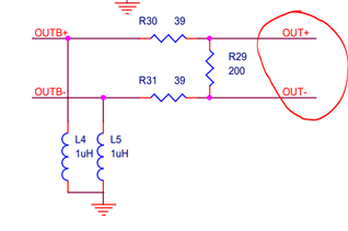
    2. Is the schematic attached is complete or Partial. Reason I am asking is I dont see OUT+ and OUT- nets connected any where.

    To debug if everything is as expected on board, First lets start with DC, Remove R30,R31,R32,R33 and L2,L3,L4,L5 must be installed, Then measure Input and Output DC voltages on both channel A and Channel B while the +5V supply is ON. Do note that you don't need to give input signal for this experiment

    Regards,
    Hruday


  • Dear Hruday,

      Sorry for replying so late. I debugged your comments. After removing R30, R31, R32, R33, the input DC voltage of the A and B channels tested was 2.447V, and the output DC voltage of both the A and B channels was approximately 0V. Is this normal? Also, sorry due to my negligence, I provided you with the schematic that was not updated, connected to the Differential to Single module by checking the PCB, OUT+ and OUT-netname.

    Regards,

    Sunny

  • Hi Sunny,

          Input and Output Voltages looks good hence device is not damaged. So without changing any components on board from this state, Can you check the output by giving the Ac signal on inputs individually? You need to do in two steps to check two amplifiers. You should see outputs on both cannels now as both channels are symmetrical

    Regards,

    Hruday

  • Dear Hruday,

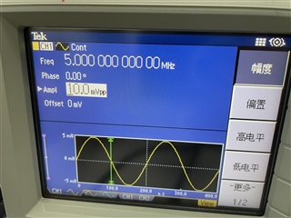
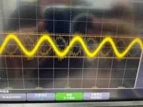
       Thanks for your patient guidance, the no output issue has been resolved. But now there is a new problem, the output signal is distorted. The signal generator setup is shown in Figure 1, and the oscilloscope shows severe distortion. I tried replacing R34, R35 with a 0.1uF capacitor and the distortion remained. The oscilloscope displays the results as shown in the next two figures.

    Regards,

    Sunny