This thread has been locked.

If you have a related question, please click the "Ask a related question" button in the top right corner. The newly created question will be automatically linked to this question.

TLC2652A: LinCMOS feature

Part Number: TLC2652A
Other Parts Discussed in Thread: TLC2652, OPA182

Hello,

I'm seeing datasheet of TLC2652A. I notice that arch of this device is LinCMOS.
It seems even though this device has kind of "CMOS" process, input bias is very low.

I'm interesting in difference between LinCMOS and standard CMOS.
Is there any document which is described difference between above two ?

Best regards,

  • Hi Ryuuichi,

    I believe the LinCMOS was the name used in early 1990's for silicon-gate process technology to differentiate it from the conventional (at the time) metal-gate CMOS processes used for digital circuitry.  However, nowadays all analog CMOS processes use silicon poly-gate technology therefore, there is little difference between them and old LinCMOS. 

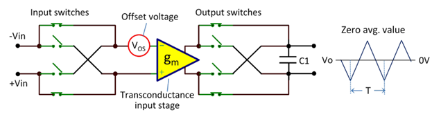
    Having said that, all CMOS processes have very high input impedance (in the range of 1Tohm); thus, their input bias current, IB, is in the pico-Amp [pA] range or lower.  However, TLC2652 is a chopper stabilized op amp, which auto-corrects its own offset by using front-end switches to reverse polarity of the offset - this results in few nano-seconds IB spikes coming from closing/opening the switches that integrated over time result in the increased IB current in the range of 100pA.

  • Hello Lis-san,

    Thank you for your reply.
    I think that "chopper stabilized op amp" mean same as current "zero-drift op amp".
    So, I understood that this tech reduces change of offset voltage (keep low value for offset drift) but not describe for bias current.
    according to your reply, I think above my understanding is a little bit incorrect but do you think so ?

    Best Regards,

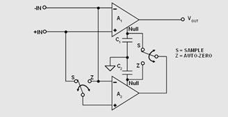
  • The zero-drift op amps include two topologies:

    1. chopper-stabilized op amps shown below:

    2. auto-zero op amps where capacitor is pre-charged with the offset voltage and then used to calibrate it out - see below:

    For more details, please read the short article attached below.

    Vos Internal Calibration.pdf

  • Hello,

    Thank you for your reply and sending document.
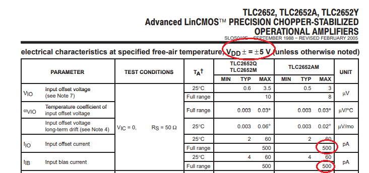
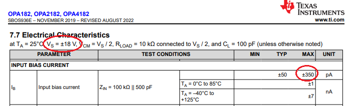
    Now, I'm comparing TLC2652A and OPA182. As you mentioned, max IB of TLC2652A is 100's of pA(150pA). However, max IB of OPA182 is "nA"(7 nA) order.
    From your document, I believe that max IB of OPA182 expect simlar value with TLC2652A, but value is different in fact.
    Is it expected result ?

    Best Regards,

  • Machida-san,

    In comparing TLC2652 and OPA182 input bias current (IB) you must consider supply voltage and operating  temperature.

    At room temperature, IB in both op amps is comparable as it is dominated by the integrated value of the current spikes coming from chopping action of the op amps front-end.  However, at the elevated temperature (especially above 85C), the leakage current of the reverse-biased ESD protection diodes dominates the IB magnitude.  Since the supply voltage used for TLC2652 is only +/-5V while for OPA182 is +/-18V, the reverse-bias voltage across the ESD protection diodes of OPA182 is much higher resulting in higher IB at high temperature - see below.

  • Hello Lis-san,

    Sorry for my late reply.
    At first, I thought even though input arch is same, why this big difference appear. However I almost understand the reason.

    If user will use same VDD as TLC2652A(+/-5V), will IB spec of OPA182 be close to TLC2652A ?
    (In general, which one small VDD or large VDD do become small IB spec ?)

    Best Regards,

  • Hi Machida-san,

    In general, the lower supply voltage results in a lower reverse-bias leakage current across the Input ESD protection diodes and thus lower IB.  I do not have IB magnitude of OPA182 on +/-5V supply at gugh temperature, thus I cannot tell you what exact IB magnitude it will have but I’m sure it will be much lower than under +/-15V conditions listed in data-sheet.