This thread has been locked.

If you have a related question, please click the "Ask a related question" button in the top right corner. The newly created question will be automatically linked to this question.

INA851: Current sensing using INA253 and INA851

Part Number: INA851
Other Parts Discussed in Thread: INA253, TINA-TI, REF3425

Hi TI,

I have a requirement for low side current sensing design for the current range of -10A to +10A , with differential output. The current sense circuit should be able to measure upto 5mA resolution. For this i have chosen INA253A2 as my current sense amplifier with ref 2.5V and the output of the INA253A2 and ref voltage is fed to the INA851 instrumentation amplifier for fully differential output.

Can you please provide me with some guidance on this selection ? Would you recommend using INA253 and INA851 ?

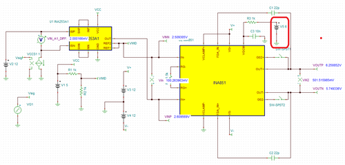
I have simulated this design in TINA TI but i'm not getting fully differential output from INA851. Images attached for your reference. Please help mein resolving this error.

Thanks & Regards,

Venkat.

  • Hi Venkat,

    What is the INA851 differential output common-mode voltage level required in the application?  Are you driving an ADC or what circuit is driven by the INA851?

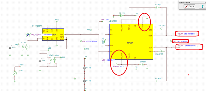
    In your circuit above, VOCM = 0V while VCLAMP- = GND, hence VOCM is outside the valid range.  Please set the VOCM to a voltage well above GND, within the VCLAMP+/- range. See example below, VCLAMP=+6V while VCLAMP+=12V and VCLAMP-=0V:

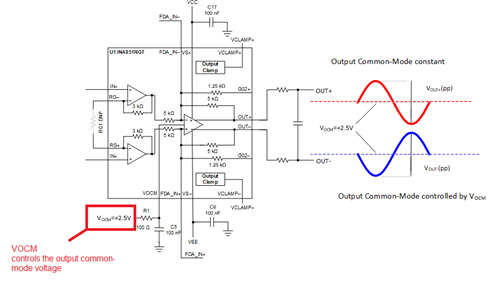
    The VOCM pin is used to set the fully differential output common-mode voltage, and this voltage needs to be set within the range of the clamp voltage supply, ideally close to the mid-clamp voltage range, but there is flexibility in the VOCM range.  The INA851 device integrates a fully-differential amplifier output stage intended to drive fully-differential circuits, where both OUT- and OUT+ voltages are allowed to swing, centered around the VOCM output common-mode voltage.  The VOCM pin controls the output common-mode voltage.  For example, if VOCM is set to +2.5V, both VOUT- and VOUT+ produce a  fully-differential signal centered at +2.5V:

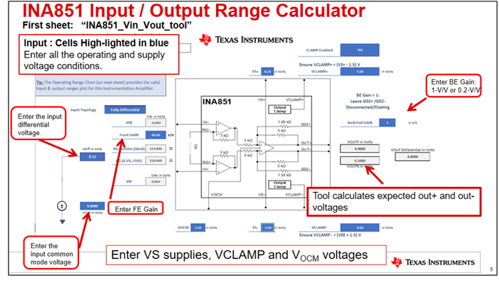
    We also offer an excel calculator to verify/check the device is inside the input/output linear range.  

    Regarding the INA851 Input voltage range Calculator (excel) tool:

    You can download the excel tool on the link below and verify the amplifier is in range:

    INA851 Input-Output Range Design Calculator

    Attached is a pdf document with instructions:

    INA851 Input and Output Range Design Calculator Instructions.pdf

    Also, it was explained to me that the INA851 TINA-TI/PSPICE model is preliminary, and there may be limitations simulating the clamping functionality.  The SPICE model is in the queue pending a revision.  Nevertheless, let me know your VOCM voltage requirements, and we can check the circuit for you.

    Thank you and Regards,

    Luis

  • Hi Luis,

    Thanks for your quick response.

    What is the INA851 differential output common-mode voltage level required in the application?  Are you driving an ADC or what circuit is driven by the INA851?

    My differential output will be driving an ADC which supports a differential input of  +/-10V.

    Based on the above spec, what can be my VOCM to be set ?

    One more doubt -

    Can i get purely differential output, For example : In your circuit VM2 is 500mv, can i get VoutP- +250mV and VoutN- -250mV ? (This should apply for any  value of VM2). Because i have to feed these signals transimitted through cable to the ADC in remote. To minimise the noise interference, i have chosen fully differential amplifier.

         Even your circuit is not giving actual differential signals. Please explain me if my understanding is wrong.

    Thanks & Regards,

    Venkat.
  • Hi Venkata,

    The INA851 output VOCM voltage will need to be set according to the input common-mode requirements of your ADC.

    It is clear the ADC you support requires a differential input of +/-10V.  What is the actual input common-mode voltage requirement of your ADC

    For example, your ADC is powered with bipolar supplies, ±12V , and the fully-differential signal ( +/-10V) swings around GND = 0V or a common-mode voltage of 0V,.in this case, the VOCM will need to be set to 0V.  

    Another example, if your ADC is powered with a unipolar supply, +12V and GND and let's say, the ADC requires fully-differential signal ( +/-10V) that swings around +6V.  In this case the VOCM needs to be set to +6V.

    Can i get purely differential output, For example : In your circuit VM2 is 500mv, can i get VoutP- +250mV and VoutN- -250mV ? (This should apply for any  value of VM2). Because i have to feed these signals transimitted through cable to the ADC in remote. To minimise the noise interference, i have chosen fully differential amplifier.

         Even your circuit is not giving actual differential signals. Please explain me if my understanding is wrong.

    The INA851 iintegrates a fully-differential amplifier output stage, hence the INA851 circuit is completely fully-differential. 

    As any fully-differential amplifier output signal, the output is centered around the VOCM common-mode voltage level. The output voltage is also limited by the VCLAMP+/- voltage.  The INA851 output voltage is of course also a function of the input voltage you feed into the device, as well as the VOCM voltage.

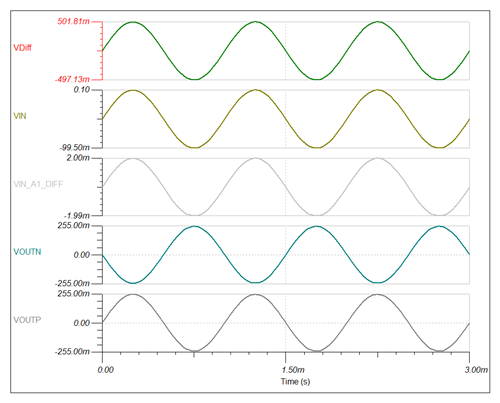
    If you require the absolute value of VOUTP+=+250mV and VOUTN=-250mV, then VOCM must be set to GND or 0V, and VCLAMP- needs to be set to a negative voltage, below the most negative output swing voltage to allow enough headroom for the signal as specified on the INA851 datasheet.  See example below:

    Below is the transient response.

    Best Regards,

    Luis

  • Hi Luis,

    your explanation was very clear and understood the concept.

    One more doubt, In Tina TI how to set the resolution of the voltmeter and ammeter ?

    In my application, voltmeter and ammeter is showing readings up to two digits only (for example :2.53V), but in your image the readings are up to 5 digits after decimal. Can you just help me out in setting the resolution ? This doubt is not related to the INA851 but it would be very much helpful for me.

    Thanks & Regards,

    Venkat.

  • Hi Venkat,

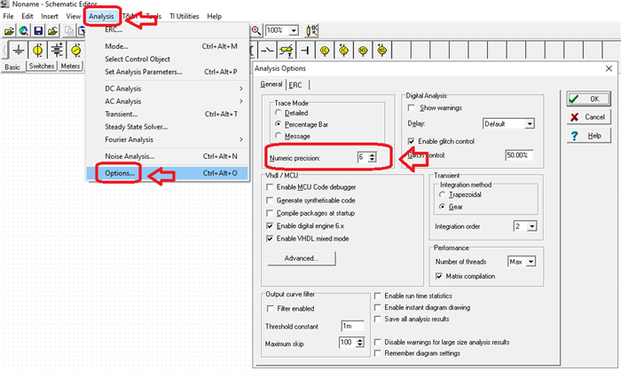
    On TINA-TI, on the top menu, please click on "Analysis" , and  "Options" and the "Analysis Options" tab opens, on the "Numeric precision" field, select "6" for six digit precision:

    Let me know if you need anything,

    Thank you and Best Regards,

    Luis

  • Hi Luis,

    I have simulated the circuit using TINA TI for full scale voltages from -10A to +10A, with VOCM= +2.5V. But the simulation results itself are showing up errors. The document with simulation results for different values are attached for your reference. 

    Can you comment on this, why i'm getting these errors at the output of INA851 in simulation stage itself ?This errors may be more in real scenario.

    Can you please guide me in reducing these error values ?

    Thanks & Regards, current_sense_SIM_3.pdf

    Venkat.

  • HI Venkata,

    I need to ask you a few questions:

    1) One concern is the pdf document shows a comment:  "System Gain error: ±0.05%" : Is this the max gain error allowed in the application or a typical? What is the max gain error target on this application?  Keep in mind,  in most current shunt measurement applications, the shunt resistor tolerance dominates the gain error in the measurement.  The INA253 offers good accuracy with shunt resistor tolerance of ±0.1% max. The expected gain error of the INA253A2 is ±0.05 typical and ±0.4% max.   

    Just the expected typical 0.05% gain error of the INA253A2 can cause an error exceeding 10mV in this circuit which explains the result.  Hence it is not surprising to see total output system errors exceeds 10mV in the circuit.

    2) On the real application circuit, what is the tolerance and drift of the RG resistor that you plan to use?    The gain error of the INA851 is ±0.2% maximum primarily due to the mismatch of the RG external resistor to the internal resistors of the INA.  This specification assumes a high precision, low drift  RG resistor offering  better than 0.1% tolerance is used. 

    3)  How are you calculating gain error of the system on the pdf document that shows the simulation results? Are you substracting the system offset error prior calculating gain error? Or displaying the absolute total error combining all offsets and gain errors involved in the system? 

    - What is the input common-mode voltage at the INA253A2 in the application?  The simulation shows a floating current source at the INA253A2 input, where the common-mode voltage is not properly defined.  Can you share the simulation, and also let me know the input common-mode voltage?

    The TINA simulation will only provide typical error results but not maximum.

    Thank you and Regards,

    Luis

  • Hi Luis,

    Apologies for the delayed response.

    2) On the real application circuit, what is the tolerance and drift of the RG resistor that you plan to use?    The gain error of the INA851 is ±0.2% maximum primarily due to the mismatch of the RG external resistor to the internal resistors of the INA.  This specification assumes a high precision, low drift  RG resistor offering  better than 0.1% tolerance is used. 

     => Luis, I'm planning to use resistor of 1.5Kohms of tolerance +/-0.1% for RG in INA851. This design will be used in Lab environment.

    Is the tolerance is sufficient for minimum error output ?

    3)  How are you calculating gain error of the system on the pdf document that shows the simulation results? Are you substracting the system offset error prior calculating gain error? Or displaying the absolute total error combining all offsets and gain errors involved in the system? 

    => Please ignore the error mentioned in the document. Can you guide me in calculating overall gain error including both INA253 and INA851 ?

    4) What is the input common-mode voltage at the INA253A2 in the application?  The simulation shows a floating current source at the INA253A2 input, where the common-mode voltage is not properly defined.  Can you share the simulation, and also let me know the input common-mode voltage?

    Luis, In my application An external power source of 12V to 16V is driving a load, my requirement is bidirectional low side current sensing. Can you guide me how to determine the common mode input voltage for the INA253 ? I'm little bit confused with this.

    Thanks & Regards,

    Venkat.


  • HI Venkata,

    1) In general, using the INA851 with 0.1% tolerance resistors with 20ppm/C drift will offer very good performance.

    Using the root sum of the squares, we can add uncorrelated errors to obtain an estimate of error.  For example, the INA851 datasheet specifies a max error of 0.2% (for G>10).  An approximate estimate of INA851 worst case gain error, assuming 0.1% tolerance resistors at room temperature is:

    GE = sqrt((0.1%)^2+(0.2%)^2) = ~±0.22%   (Estimate of max gain error at room temperature, based on max gain error spec, assuming 0.1% resistor tolerance)

    The typical INA851 gain error is lower.  Figure 7-13 of the INA851 datasheet, shows a plot of the typical gain error histogram of the INA851, with a standard deviation of ~0.0136% and mean of ~-0.0048%., therefore the INA851 typical gain error is around 0.0154%.  Hence, the INA851 gain error is in most cases dominated by the resistor tolerance. If you were assume the resistor distribution has a standard deviation error around ~0.033%, the typical INA851 gain error would be around ~±0.04% using the root-sum-of-squares calculation:

    GE = sqrt((0.0154%)^2+(0.033%)^2) = ~±0.04%   (Estimate of typical INA851 gain error at room temperature)

    2) The INA253 datasheet specifies a system gain error of ±0.05% typical, ±0.4% maximum.

    You can use the RSS to combine the INA253 and INA851 gain error to obtain an estimate of circuit gain error:

    GE(INA253+INA851) = sqrt((0.4%)^2+(0.22%)^2) = ~±0.46% (Estimate of gain error at room temperature, based on max spec)

    GE(INA253+INA851) = sqrt((0.05%)^2+(0.04%)^2) = ~±0.06% (Estimate of gain error at room temperature, based on typical)

    I used the root-sum-of-squares for the estimates above; although other more conservative estimates sum all errors directly.  Nevertheless, I find that using the root sum of squares method provides a much more realistic estimate of error. This is because the compounded probability that all the devices above have an error near maximum simultaneously is very small.

    The quick example above provide a gain error estimate at room temperature, and do not account for gain error temperature drift, as well as the offset errors and common-mode voltage errors in the system.  The tutorial below discusses combining the errors of a current shunt amplifier, an op-amp and an ADC, to calculate total-uncalibrated error of a circuit.  It provides a useful discussion of the statistics behind error analysis:

    Statistics behind error analysis of ADC system

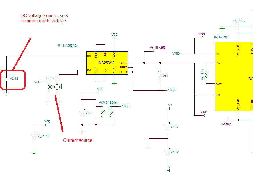
    3) On your simulation circuit, you can define the common-mode voltage with a DC voltage source, and use a current source to set the current through the shunt resistor:

    Thank you and Regards,

    Luis


  • Hi Luis,

    Thanks for the great explanation.

    What is the maximum current consumption of VOCM, VS+ and VS- pins of INA851 ?

    Regards,

    Venkat.

  • HI Venkata,

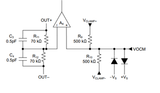
    The VOCM has a ~250kΩ input impedance or 500kΩ-500kΩ voltage divider.  Hence, the input current into VOCM will vary with the input voltage applied into the voltage divider. 

    The supply quiescent current with VIN=0 and no load is 7mA max at 25C, and 9mA max over the -40C to +125C temperature range.  As any other  instrumentation amplifier, the supply current will increase as you load the output of the circuit and/or apply different amplitude signals over frequency.

    Thank you and Regards,

    Luis

  • HI Luis,

    Is there any equations available for the exact current consumption of INA851 for a particular VS+ , VS- and VOCM voltages because i have to use 16 INA851s in my design and i have to do power budgeting of each rail.
    My inputs will be : 

    Input : -/+ 5V

    VOCM : +2.5V

    VS+ & VS- : +12V & -12V respectively.

    Vclamp+ and Vclamp- : clamping disabled (shorted to VS+ and Vs-)

    out+ and out- : +/-10V

    The output will be driving an ADC which is in Remote.

    My Questions are : 

    1) Can you please guide me in calculating current consumption of INA851 on each voltage rail as per the above inputs (as this information is not mentioned in Datasheet) : 

        a)  Iocm (current consumption on VOCM rail as i have to choose a Ref voltage generator IC

              For now i have chosen one REF3425 to source one  INA253A2 and one INA851

        b)  Is+ and Is- (current consumption on Vs+ and Vs- rail separately as both are powered by different sources) 

    2) What is the driving capacity of INA851 in terms of current for above mentioned input ? because graphical observations are given for only above 12V. 

    FYI : The output will be driving an ADC which is in Remote.


    Thanks & Regards,

     Venkat.

  • HI Venkat,

    Regarding the VOCM, this is a  500kΩ-500kΩ voltage divider to the Vclamp pins that can be solved using fundamental/basic circuit analysis. If you have the clamps set at ±12V, then the VOCM when left floating is biased at GND (0V).  When using the REF3425 (2.5V), the nominal current consumption is ~10uA (+2.5V / 250k =~10μA.

    No special equations are available to resolve the current consumption of the INA851.  Similar to any other amplifier, the current consumption will be a function of the INA851 quiescent current plus any current consumption on the load.  The INA851 quiescent maximum current consumption through the input supplies is 9mA, on the supply pins plus any current consumption on the load of the circuit. The quiescent clamp pins current consumption is ±80uA max respectively

    Most ADCs have relatively high input impedance and don't consume 10's of milliamps at the inputs. Depending on the ADC input structure architecture, the input may have a RC sample-and-hold structure.  Other ADCs incorporate an amplifier buffer input.  In general, ADCs inputs consume average currents in the microamp range (or less).  Not sure what is meant by remote.  When driving precision ADCs, in general, the driver amplifier is kept in close proximity to the ADC.  This can be particularly important for ADCs that have unbuffered inputs, where the amplifier has to drive an unbuffered sample-and-hold and settle within the resolution of the ADC.

    Regards,

    Luis