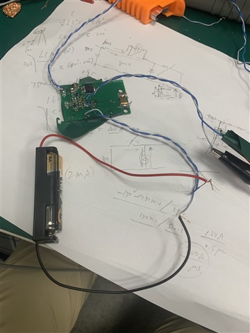
This thread has been locked.

If you have a related question, please click the "Ask a related question" button in the top right corner. The newly created question will be automatically linked to this question.

OPA365-Q1: how to layout a high speed opamp to avoid oscillation

Part Number: OPA365-Q1

Hi,

I laid the PCB of an OPA365-Q1 according to the suggestions I collected from TI’s related documents.

  1. Good power supply decoupling
  2. Keep inverting pin as small as possible
  3. Remove the ground under the inverting pin.

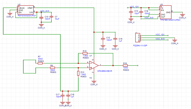
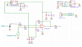
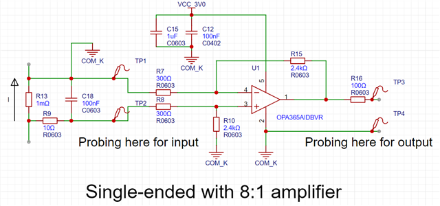
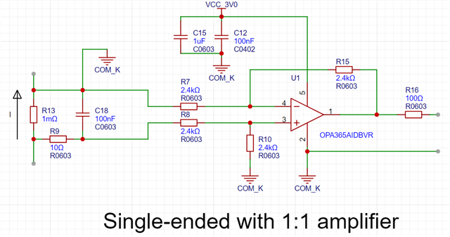
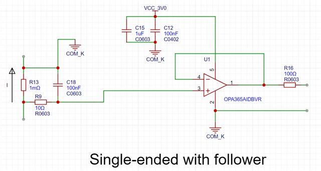
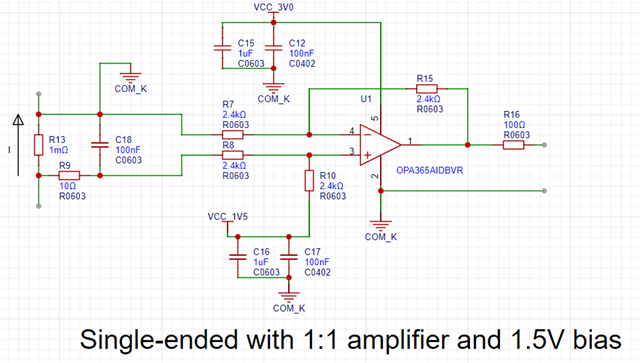
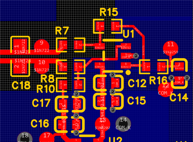
See below figure for my layout at the opamp. U1 is the opamp. R7 and R15 is a voltage divider at inverting pin. R8 and R10 is a voltage divider at non-inverting pin. C12, C15 are decoupling capacitors on its 3V power supply pin. C16 and C17 are capacitors for its 1.5V DC bias. Red traces are on top layer. Blue background is ground on bottom layer. This is a two-layer board of thickness 1.6mm.


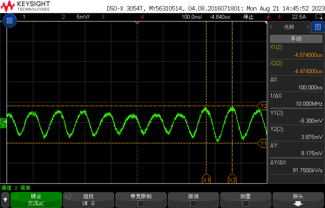
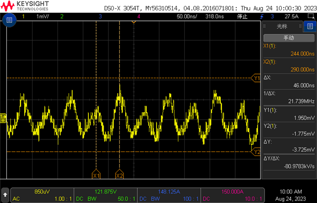
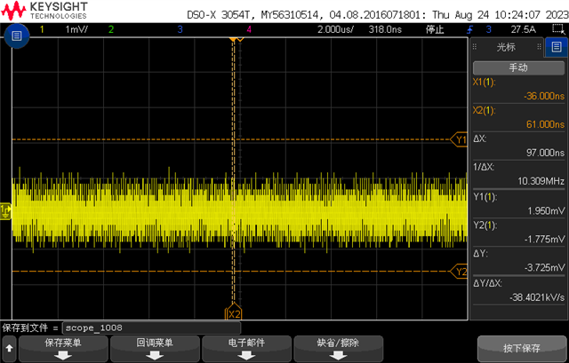
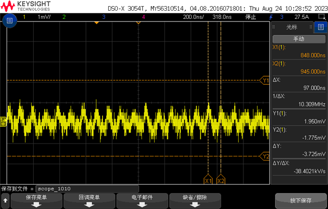
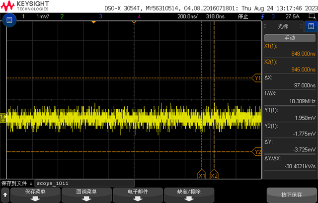
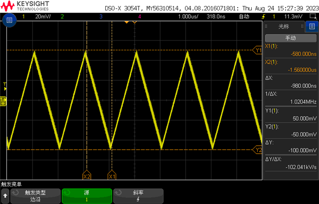
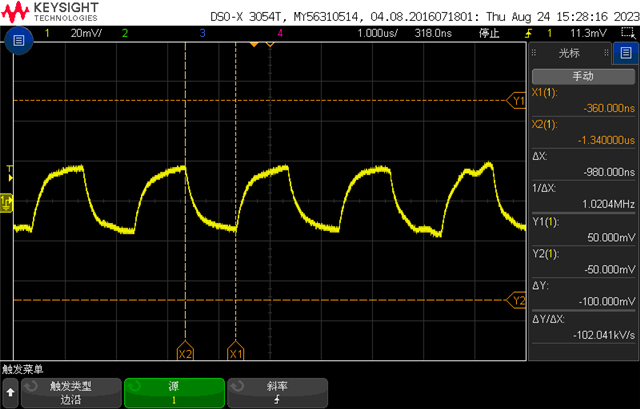
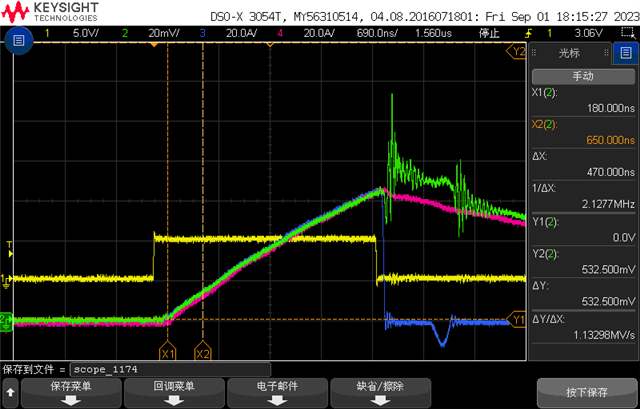
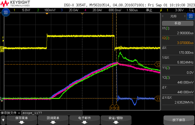
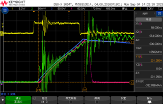
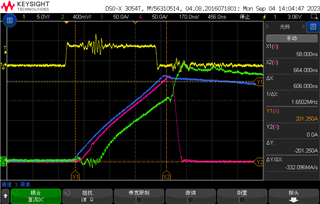
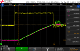
After experiments with this board, I have the oscillation (around 10MHz) at the output when the input is short-circuited (which means no input signal is added). What’s wrong with my PCB layout?

  • Hi Xuejun,

    Can you please also share the schematic showing the resitor and capacitor values?

    Regards

    Anant

  • Yes, of course. Below is the schematic of this circuit. Before R7 and R8, there are some components but I short circuited the input just at this point.

  • Hi Xuejun,

    What is the value of C14 which in layout is connected after (right hand side) R16? Is any component other than this cap connected there?

    You mentioned that there are some components before  R7 and R8 which you shorted? what are those component? Is that node which you shorted driven by some other component or is that a high-Z or floating node?

    Regards

    Anant

  • Hi Anant,

    I omit those components just want to make clarification easier. C14 actually is not installed current shunt R13 and its related compensation Rs and C are not installed. The shorted node at input of R7 and R8 is a floating node.

  • Hi Xuejun,

    There is couple of things you can try

    1. You can reduce down the resistor value of R15/R10 and R7/R8, keeping the ratio same. Say for example 750ohm and 3Kohm instead of 7.5Kohm and 30Kohm. This should help in stabilizing. The reason for this is 7.5KOhm Fb resistor along with the input capacitance will bring the 2nd pole close to 8-10Mhz. This can cause instability so changing it to 750Ohm will push the 2nd pole beyond the UGB  and hence will help.

    2. Or alternatively, you can connect a small feedback capacitor (few 10s of pF based on your bandwidth requirement) in parallel to R15 ( you may need connect the same value capacitor across R10 aswell to keep the impedance ratio same at high freq).

    Regards

    Anant 

  • Hi Anant,

    Thanks for your tips. I tried 3kOhm/750Ohm and 1.2kOhm/300Ohm with 20pF feedback capacitor. The 10MHz oscillation is very stubborn and still show its presence. See below pictures for test results.

    • With 3kOhm/750Ohm and 20pF capacitors

    • With 1.2kOhm/300Ohm and 20pF capacitors

    From the test results it is clear that the noise amplitude is reduced from +/-5mV to +/-2mV and at last to +/-1mV. But the 10MHz oscillation is also clear to be present. For reference, the background noise is also about +/-1mV, but with no obvious oscillation pattern. See below figure.

    What else can I do then?

  • Hi Anant,

    I go further with this opamp even we are still left with some 10MHz oscillation at the output.

    I want to check the opamp's reaction to input common mode voltage. Due to the configuration of attenuator of 1:4, I think I have some common mode voltage capability.

    With a signal generator of 50Ohm resistance connected to the input and the signal of a triangular shape with peak to peak of 400mV and frequncy of 500kHz, the output waveform looks like below, which is quite good and as expected.

    However, when I connect a one battery of 1.5V to between its inverting input (before R7, not inverting terminal of the opamp) and ground, the output waveform is distorted like below.

    Just for your reference, below picture shows how I connect one 1.5V battery.

    My question is what happens with the opamp. How it behaves like this? What's wrong with my experiment?

  • Xuejun,

    Can you please confirm if this the correct representation of your setup or not?

    Regards

    Anant

  • Hi Anant,

    No, the triangular signal is added between R7 and R8 and it has an output impedance of 50Ohm. The 1.5V battery connection is right.

  • Xuejun,

    Can you capture the waveform at the output of the signal generator (triangular wave) after you connected the battery? Please do it in DC coupling mode of oscilloscope so that we can see the added DC offset also.

    Regards

    Anant

  • Hi Anant,

    I have found and solved the issue. The issue is with the generator itself. When I add the common mode voltage and touch the circuit ground with the single-ended probe ground tip, the generator output will get distorted. The solution is to use a signal transformer to isolate the generator output which my lab happens to have. Thanks for your support. 

    Do you have additional recommendation on the residual +/-1mVp-p 10MHz oscillation suppression?

  • Xuejun,

    I don't think this +/-1mVpp oscillation is because of device unstability. Can you probe the gnd and both the supply (Vcc and VEE) to check if that osillation is present there also?

    Regards
    Anant

  • OPA365 test results.pdf

    Hi Anant,

    See attached file for test results. Yes. I noticed that the voltage across a 1nF extra decoupling MLCC on top of the Opamp is not good. When this 1nF decoupling capacitor is not there, there will be spike like noise on the supply pin. I guess the left oscillation is due to bad power supply decoupling. But I am wondering how I could improve this power supply decoupling. One aspect I could see is to use a four layer board to decrease the inductance cause by board thickness. Do you have other ideas on improvement of this decoupling thing?

  • HI Xuejun,

    You can add multiple decoupling capacitor in parallel like 10nF, 100nF, 1uF, 10uF. Also having a good ground plane is important for optimum performance.

    Regards

    Anant 

  • Hi Anant,

    Thanks. Actually I want to ask if you have some successful layout pattern for such SOT23-5 high speed opamp.

    New issue occured with this opamp. See below description. Only focus on the linear ramp up part on the waveform and neglect the wild oscillation part.

    I have the opamp in single-ended configuration without 1.5V bias, with 300Ohm/2.4kOhm resistive dividers as an 8:1 amplifier. I have the input voltage waveform as below green trace. If follows the current waveforms (blue and purple traces) very well.

    However, the opamp output waveform looks like below green trace. All traces are with DC coupling. 

    You could see that the output trace has large distortion from very beginning (around 0 volts) and some time delay (around 170ns) as a whole. 

    I used below 1:1 passive probe for these two green traces. Once for input signal and once for output signal. Output trace is probed after one 100Ohm resistor at the opamp output terminal.

    What happens with the opamp? I think the slew rate here is not large, only calculated to be 480mV/3us=0.16V/us.

    Is the distortion around zero volt due to imperfection of opamp and the delay due to the bandwidth limit of high gain? What can I do to improve on such situation?

  • Xuejun,

    R7/R8 is 300Ohm and R10/R15 is 2.4KOhm, correct?

    Regards

    Anant

  • Hi Anant,

    Yes. See below figure for the circuit.  R9 and C18 is there for frequency compensation of current shunt R13 voltage output.

    I have also tried below configurations. All have similar output limitations.

  • Xuejun,

    I believe the green waveform in the first graph is for TP2, can you share the waveform for TP1 aswell.

    Also please can you capture TP1/TP2 and output waveform using a higher bandwidth probe (atleast 50Mhz) and with lesser input capacitance.

    Regards

    Anant

  • Hi Anant, 

    Green waveform is probed between TP1 and TP2, with TP1 as reference. Output is captured similarly between TP3 and TP4, with TP4 as reference.

    Previous information I gave is misleading. For different configuration I tried, actually I used fast switching and the input waveform is oscillating near zero volt, so the output is delayed quite a lot. See below figure for input.

    See below figure for output.

    When I slowed down the MOSFET switching on speed, the input oscillation is suppressed. In combination with using opamp configuration as a 1:1 amplifier, I could make the output waveform follow current waveform very well. See below figure.

    So I should say this issue is solved.  When other issues pop out, I will let you know.

    Thanks a lot.

  • Yes definitely, let me know if you have any other query