Part Number: LMP7721
Other Parts Discussed in Thread: OPA928, OPA928EVM
Hi,
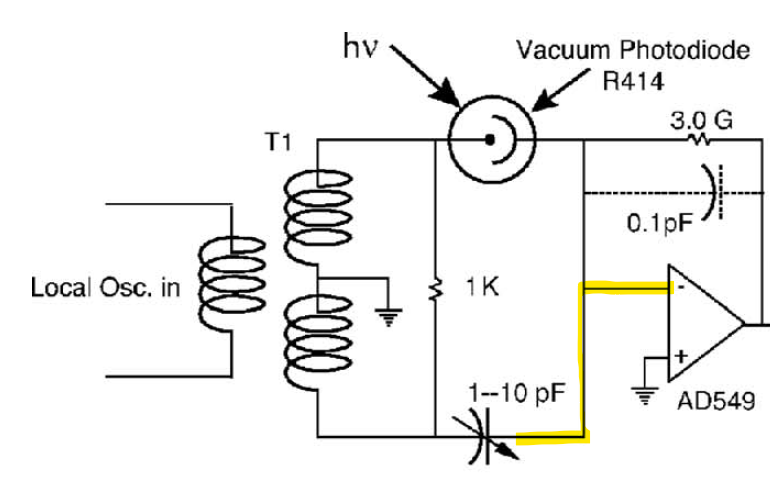
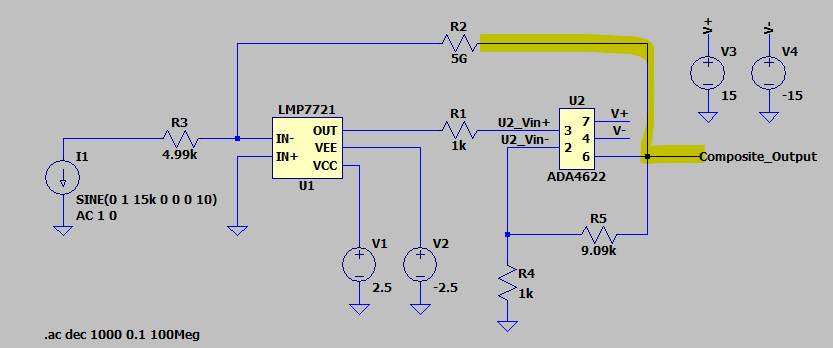
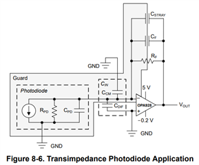
I'm working on a sensor application using a photodiode connected to a transimpedance amplifier with a 5 Gigaohm feedback resistor.
Read Paul Grohe's 2011 series of articles "Design femtoampere circuits with low leakage" but I still would like to confirm my approach.
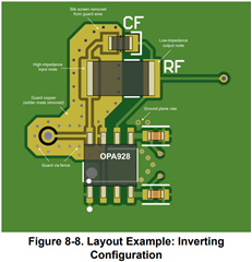
Basically I'd like to get an opinion on my layout please. The help is very much appreciated.
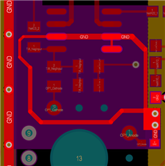
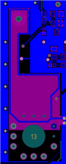
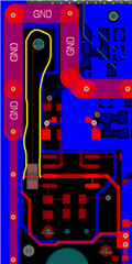
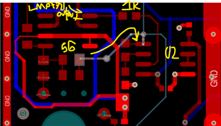
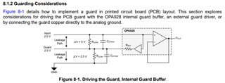
Tied the Guard to GND since that is the same potential as the +IN input. See Paul's response to a similar question here (from 9 years ago!):
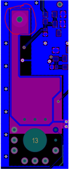
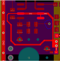
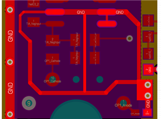
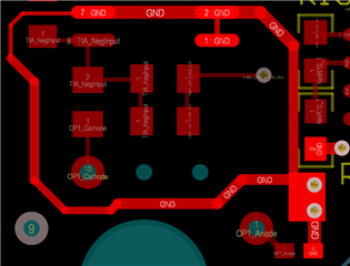
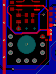
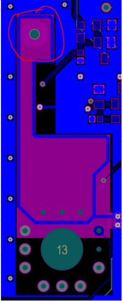
Connected the +IN input to the guard and whole thing to the ground plane using a single point. See image below.
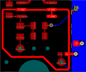
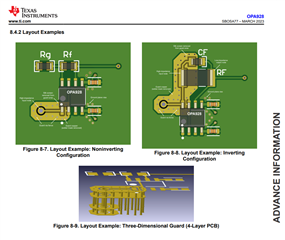
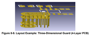
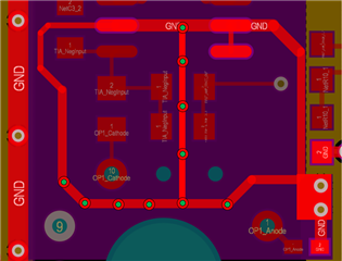
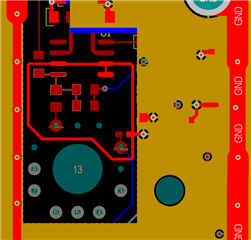
Other precautions were to remove the copper pour under the sensitive area on all layers (this is a 4 layer board) and also remove the soldermask on the critical area on both sides:
The photodiode has a round footprint with through hole pins, only two of them active (anode and cathode). I removed the plating and pads from the pins adjacent to active pins, to avoid bring noise in (planning to cut those unused pins). For the cathode pin I removed the plating and just left the pad on the top side, where it will be soldered. That way the pin is not soldered across the hole plating and to the other side, potentially picking up noise from there. For the anode pin I do need to take a signal out on the secondary, so I left the plating and top and bottom pads.
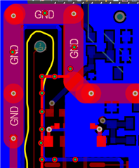
Trace widths for critical signals is 8 mils. Added the pads for feedback capacitor (0805) that I may or may not populate, based on testing results. Found ceramic capacitors with an insulation resistance of 50 Gohms, so substantially higher than the 5 Gohm of the feedback resistor. The output goes to a second stage, another op amp in voltage amplifier configuration. Around the whole thing there is a metal shield enclosure, placed along the thick GND traces. 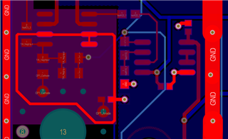
Thanks!