This thread has been locked.

If you have a related question, please click the "Ask a related question" button in the top right corner. The newly created question will be automatically linked to this question.

THS4503: GAIN LESS THAN 1

Part Number: THS4503
Other Parts Discussed in Thread: ADS1675, THS4130, TINA-TI, THS4551, THS4541

This probably applies to all the THS diff amp products.

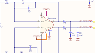
I am using the amp as an ADC input with VCOM offset as well. I have a gain less than unity and  I have heard that it can be unstabl;e with less than unity gain. I simulated it in spice and it was stable.Below is the circuit,

I did add the two feedback caps to flatten the bode plot at the knee, but otherwise it was stable. I am driving an ADS1675

  • Hello Robert,

    Could you share your test parameters (input signal type, frequency, amplitude, etc)?  Are you simulating stability via a stability analysis, or are you observing the stability of the system by looking for gain-peaking and overshoot?

    Do you have concerns about your circuit being stable, or a general request to examine if a circuit with a gain less than unity can be stable?

    You do appear to already be using series resistors at the output of the amplifier network, which would work as isolation resistors in a stability solution.

    Best,

    Alec

  • I performed a complete system simulation and looked for gain peaking as you say. Here is my LTspice and netlist

    How can I send the LTSpice circuit file?

    * C:\SPICE\CIRCUITS\cyrus input cct bode plot.asc
    XU1 N001 N007 oa N005 N006 DMOD8599
    XU2 N009 N015 ob N012 N014 DMOD8599
    V1 N001 0 +5.0
    V2 N013 0 1.5
    V3 N009 0 +5.0
    V4 N015 0 -5.0
    R1 N006 N014 10k
    R2 N005 ia 33
    R3 N012 ib 33
    R4 N002 oa 3k24
    R5 oa N006 1k
    R6 ob N014 1k
    R7 N008 ob 3k24
    R8 ia ib 2k
    R9 ib N010 3k16
    R10 ia N004 3k16
    R11 adcp N003 10
    R12 adcn N011 10
    C1 adcp 0 100p
    C2 adcn 0 100p
    C3 adcp adcn 750p
    R13 adcp adcn 40k
    R14 N003 N002 2k
    R15 N011 N008 2k
    C4 N003 N002 47p
    C5 N011 N008 47p
    V6 N007 0 -5.0
    C6 adcp adcn 12.5pF
    XU4 N002 N013 N001 N003 N011 N015 N001 N008 THS4130 THS4130
    R16 N004 0 500k
    R17 0 N010 500k
    V7 N004 N010 AC 1
    C7 oa N006 22p
    C8 ob N014 22p
    .SUBCKT DMOD8599 7 4 6 3 2
    * Input Impedances
    G3 3 2 3 2 82U
    R1 3 0 1.6G
    R2 2 0 1.6G
    C1 3 0 2.25P
    C2 2 0 2.25P
    C3 3 2 7P
    * Input Clamping
    D1 3 12 D1
    D2 12 2 D1
    D3 2 13 D1
    D4 13 3 D1
    .MODEL D1 D IS=1E-16
    * Preconditioning Gain Stage and Sum Node for Gain Control
    * and Noise Insertion
    E1 20 19 3 2 100
    R3 19 0 10M
    * Second-Order Frequency Shaping
    R50 20 21 10
    C50 21 0 110P
    R51 21 22 50
    C51 22 0 17P
    R52 22 23 250
    C52 23 0 17P
    R53 23 40 1.25K
    C53 40 0 11P
    * Limiting Amplifier with Slew-Rate Control
    G4 41 0 40 0 100U
    G5 41 0 41 0 5U
    D5 42 41 D2
    D6 41 43 D2
    V1 0 42 460
    V2 43 0 460
    .MODEL D2 D IS=1E-16 EG=0.6
    * Primary Gain Block, Dominant Pole/Zero and Swing Limiting Network
    G6 44 0 41 0 10U
    G7 44 0 44 0 33.3N
    C4 44 48 310P
    R4 48 0 60
    D7 44 46 D2
    D8 47 44 D2
    E2 46 0 POLY(1) 7 0 -1.76 1
    E3 47 0 POLY(1) 4 0 1.95 1
    * Output Stage and Gain-Reduction Feedback
    M1 7 44 45 4 MN AD=0 AS=0 L=1U W=4700U
    M2 4 44 45 7 MP AD=0 AS=0 L=1U W=4700U
    R6 45 6 1M
    G8 19 0 45 6 1000
    R5 44 50 180
    C5 50 6 400P
    .MODEL MN NMOS LEVEL=1 KP=2E-5 PHI=1.0 VTO=-120M GAMMA=0 LAMBDA=0
    .MODEL MP PMOS LEVEL=1 KP=2E-5 PHI=1.0 VTO=120M GAMMA=0 LAMBDA=0
    * Quiescent Supply Current
    R7 7 4 52K
    I1 7 4 3.53M
    ;
    ; Noise Modeling
    D60 60 0 DN1 1000
    I60 0 60 1M
    D61 61 0 DN4
    I61 0 61 1U
    D62 62 0 DN3
    I62 0 62 1U
    D63 63 0 DN2
    I63 0 63 1U
    G60 3 0 61 60 .00018
    G61 2 0 61 60 .00018
    G62 3 2 62 60 .000092
    G63 19 0 63 60 700
    .MODEL DN1 D IS=1E-16
    .MODEL DN2 D IS=1E-16 AF=1 KF=1.05E-17
    .MODEL DN3 D IS=1E-16 AF=1 KF=2.8E-17
    .MODEL DN4 D IS=1E-16 AF=1 KF=4.5E-17
    .ENDS DMOD8599
    ;tran 10m
    * VIN
    * VIN (1 +2R5/R1)
    * 3V
    * VIN(1 +2R1/R5) = 3.0\nVIN = 3/(1+2R1/R5)
    * VIN = 2.5V = 10*R8/(2R10+R8) \nR10=1.5*R8
    * Investigate the effect of the series R and also I/P Z of op-amp
    * THS4130
    *****************************************************************************
    * (C) Copyright 2013 Texas Instruments Incorporated. All rights reserved.
    *****************************************************************************
    ** This model is designed as an aid for customers of Texas Instruments.
    ** TI and its licensors and suppliers make no warranties, either expressed
    ** or implied, with respect to this model, including the warranties of
    ** merchantability or fitness for a particular purpose.  The model is
    ** provided solely on an "as is" basis.  The entire risk as to its quality
    ** and performance is with the customer.
    *****************************************************************************
    *
    ** Released by: WEBENCH(R) Design Center, Texas Instruments Inc.
    * Part: THS4130
    * Date: 10/31/2013
    * Model Type: All In One
    * Simulator: Pspice
    * Simulator Version: 16.2
    * EVM Order Number: N/A
    * EVM Users Guide:  N/A
    * Datasheet: SLOS318H-MAY 2000-REVISED MAY 2011
    *
    * Model Version: 2.0
    *
    *****************************************************************************
    *
    * Updates:
    *
    * Version 1.0 : Release to Web
    * Version 2.0 : Improving output swing vs. supply
    *               Improving common mode input range
    *
    *****************************************************************************
    * Notes:
    *   1- This macromodel predicts well: DC, small-signal AC, noise,
    *      , and transient performance under a wide range
    *      of conditions.
    *   2- This macromodel does not predict well: distortion
    *      (harmonic, intermod, diff. gain & phase, ...),
    *      temperature effects, board parasitics, differences
    *      between package styles, and process changes
    *
    * BEGIN MODEL THS4130
    * MODEL OPERATES FROM -40 TO +125 C
    * SOME PARAMETERS DO NOT TRACK THOSE
    * OF THE REAL PART VS TEMPERATURE
    * MODEL FEATURES INCLUDE:
    * OPEN LOOP GAIN, CLOSED LOOP BANDWIDTH (G>=2),
    * INPUT VOLTAGE NOISE WITH 1/F,
    * INPUT CURRENT NOISE WITH 1/F,
    * VOCM FUNCTION, OUTPUT SWING VS CURRENT
    * CMRR, PSRR, VOS, TCVOS, OUTPUT CURRENT LIMIT
    * OUTPUT CURRENT IS DRAWN THROUGH SUPPLY RAILS
    * OUTPUT IMPEDANCE, INPUT CAPACITANCE
    * INPUT BIAS CURRENT, QUIESCENT CURRENT,
    * SHUTDOWN, QUIESCENT AT SHUTDOWN,
    * AND SHUTDOWN ENABLE AND DISABLE TIME DELAYS.
    * END FEATURES
    *
    * PINOUT ORDER VIN- VOCM V+ VOUT+ VOUT- V- PD VIN+
    * PINOUT ORDER  1     2   3   4     5    6  7   8
    *****************************************************************************
    .subckt THS4130 1 2 3 4 5 6 7 8
    XI77 1 2 3 4 5 6 7 8 THS4130_HT2
    .ends
    .subckt THS4130_HT2 1 2 3 4 5 6 7 8
    XI82 46 46A 18 17 THS4130_Block1_HT2 PARAMS: SLOPE=35e-3
    XI83 38 NET509 18 17 THS4130_Block1_HT2 PARAMS: SLOPE=35e-3
    XI81 72A 72 18 17 THS4130_Block1_HT2 PARAMS: SLOPE=33e-3
    M52 38 62 59 63 PSW W=15e-3 L=1.5e-6
    G29 3 6 48 0 11.65e-3
    G26 12 17 47 0 550e-6
    G12 44 24 45 24 100e-3
    G23 39 42 47 0 550e-6
    G35 3 6 3 6 -15e-6
    G8 36 24 37 24 100e-3
    G22 43 41 47 0 550e-6
    G7 37 24 38 24 100e-3
    G3 22 21 15 16 150e-24
    G25 18 14 47 0 550e-6
    G11 45 24 46 24 100e-3
    M53 59 61 38 64 NSW W=15e-3 L=1.5e-6
    M50 57 50 17 17 NEN W=300e-6 L=3e-6
    M51 52 57 17 17 NEN W=300e-6 L=3e-6
    M45 51 52 17 17 NEN W=3e-3 L=3e-6
    M44 50 7 17 17 NEO W=300e-6 L=3e-6
    V58 62 58 -22.5
    V53 51 56 1.111e-6
    V52 53 17 1
    V54 47 54 70e-9
    V63 79 72A 900e-3
    V73 46A 94 1.35
    V75 38 73 550e-3
    V57 61 60 22.5
    V76 46 71 550e-3
    V72 93 38 0
    V69 66 22 50e-6
    V66 89 90 655.1e-3
    V65 77 17 0
    V31 49 48 0
    V74 NET509 95 1.35
    V70 81 91 16.15e-3
    V64 18 79 1.2
    V71 92 46 0
    Q35 3 41 40 QON
    Q40 43 44 39 QON
    Q53 70 78 77 QSN
    Q42 65 66 67 QIN
    Q43 68 21 69 QIN
    Q46 71 74 75 QIN
    Q22 3 14 13 QON
    Q47 73 74 76 QIN
    Q29 18 36 12 QON
    Q51 80 80 86 QCN
    Q49 74 74 83 QCN
    I24 3 6 1e-6
    I39 77 78 21e-6
    I47 6 3 242e-6
    I45 22 0 1.48e-6
    I40 79 65 2.1e-3
    I46 21 0 1.48e-6
    I9 0 15 100e-6
    I11 0 19 100e-6
    I44 0 89 1e-3
    I10 0 16 100e-6
    I12 0 20 100e-6
    I41 79 68 2.1e-3
    I13 3 6 1e-6
    I42 3 85 1.05e-3
    Q41 42 44 41 QOP
    Q34 6 39 40 QOP
    Q44 71 72 65 QIP
    Q45 73 72 68 QIP
    Q30 17 36 14 QOP
    Q18 6 12 13 QOP
    Q50 74 2 84 QCP
    Q48 80 81 82 QCP
    D36 89 0 DD
    D40 17 95 DD
    D39 17 94 DD
    D10 19 0 DVN
    D9 16 0 DIN
    D38 93 18 DD
    D37 92 18 DD
    D8 15 0 DIN
    D6 5 3 DD
    D7 6 5 DD
    D11 20 0 DVN
    D23 6 4 DD
    D22 4 3 DD
    E55 54 0 55 17 1
    E20 33 0 22 24 1
    E62 24 6 3 6 500e-3
    E21 42 0 6 0 1
    E22 43 0 3 0 1
    E13 35 34 28 0 60e-3
    E9 25 0 17 24 1
    E60 58 59 47 0 45
    E12 34 31 29 0 -60e-3
    E10 26 0 27 0 1
    E61 60 38 47 0 -45
    E19 32 0 21 24 1
    E54 49 0 47 0 1
    E5 17 0 6 0 1
    E8 23 0 18 24 1
    E6 18 0 3 0 1
    E68 22 35 90 0 140e-6
    E69 91 9 90 0 -28.5e-3
    E56 9 4 5 4 500e-3
    E11 31 1 30 0 310e-3
    E7 8 21 19 20 163e-3
    C64 53 51 2.5e-15
    C110 73 88 19.5e-12
    C109 87 71 19.5e-12
    C23 36 24 20e-15
    C18 23 28 1e-12
    C19 25 29 250e-15
    C31 45 24 200e-12
    C32 44 24 20e-15
    C65 53 57 160e-12
    C106 53 52 300e-12
    C20 26 30 1e-12
    C22 37 24 200e-12
    C63 18 50 3e-15
    C111 55 0 15e-15
    C62 7 0 1e-12
    C3 5 9 1e-15
    C4 9 4 1e-15
    C8 8 10 4e-12
    C9 1 11 4e-12
    R330 63 24 1e12
    R329 60 24 1e12
    R307 51 53 1e6
    R331 64 24 1e12
    R199 6 3 100e6
    R346 24 87 60
    R328 58 24 1e12
    R308 17 56 1e12
    R209 24 44 10
    R188 24 36 10
    R180 25 29 100e3
    R347 24 88 60
    R208 24 45 10
    R316 47 0 1e12
    R332 46 59 100e-3
    R354 34 35 1e9
    R187 24 37 10
    R183 0 29 10
    R309 57 53 10e3
    R317 48 0 1e12
    R310 52 53 10e3
    R313 0 47 1e12
    R312 0 54 1e12
    R353 35 22 1e9
    R340 17 75 333
    R314 0 47 1e12
    R357 6 24 1e9
    R184 0 30 10
    R185 32 27 1e3
    R348 71 73 700e3
    R339 70 69 15
    R318 48 0 1e12
    R178 6 3 100e6
    R315 47 0 1e12
    R186 27 33 1e3
    R355 31 34 1e9
    R182 0 28 10
    R341 17 76 333
    R179 23 28 100e3
    R62 0 10 100e-3
    R63 0 11 100e-3
    R181 26 30 100e3
    R306 50 18 10e3
    R351 89 0 1e9
    R338 70 67 15
    R349 55 51 100e6
    R352 0 90 1e9
    R342 82 85 200
    R345 6 83 666
    R343 84 85 200
    R360 7 18 50e3
    R51 6 2 30e3
    R197 0 4 1e6
    R344 6 86 666
    R52 2 3 30e3
    R212 40 4 5
    R176 0 5 1e6
    R191 13 5 5
    R361 21 8 1e9
    R356 1 31 1e9
    R358 9 91 1e9
    R359 9 4 1e9
    .ends THS4130_HT2
    .SUBCKT THS4130_Block1_HT2 VPLUS VMINUS VCC VEE
    + PARAMS: SLOPE = 33m
    E1 VPLUS VMINUS VALUE = { IF ( V(VCC,VEE) > 11, SLOPE * V(VCC,VEE), 0 )  }
    .ENDS
    .SUBCKT THS4130_Rout_HT2 Vin Vout VCC VEE
    Rout Vin Vout 5
    RVCC VCC 0 1G
    RVEE VEE 0 1G
    .ENDS
    .MODEL DD D
    .MODEL DIN D KF=9E-16
    .MODEL DVN D KF=1.5E-15
    .MODEL NEN NMOS KP=200U VTO=0.5 IS=1E-18
    .MODEL NEO NMOS KP=200U VTO=0.8 IS=1E-18
    .MODEL NSW NMOS KP=200U VTO=7.5 IS=1E-18
    .MODEL PSW PMOS KP=200U VTO=-7.5 IS=1E-18
    .MODEL QCN NPN
    .MODEL QCP PNP
    .MODEL QIN NPN BF=2000 RB=12.1 KF=3E-16
    .MODEL QIP PNP BF=2000 RB=12.1 KF=3E-16
    .MODEL QON NPN VAF=90 RE=3 BF=150
    .MODEL QOP PNP VAF=90 RE=3 BF=150
    .MODEL QSN NPN
    *NOISELESS RESISTOR SUB-CIRCUIT
    .subckt rnoiseless a b PARAMS: R=1k
    H_H1 c b VH_H1 {R}
    VH_H1 a c 0
    .ends
    *$
    .ac dec 100 10 10meg
    .lib C:\SPICE\MODELS\AD8599.cir
    .lib C:\SPICE\MODELS\THS4130.LIB
    .backanno
    .end

  • Hello Robert,

    Thank you for sharing; it is good to know your current method.  I would not be able to run the LTSpice file, but I could replicate it in TINA-TI or PSPICE if I could view a screenshot or description of the schematic and signaling.  

    If you use TINA-TI SPICE or PSPICE a circuit in either configuration would be ideal; otherwise I can work off of an image or text description.  Stability analyses are less straightforward when considering fully-differential amplifiers, but I will do what I can to examine it.

    In general I believe the best method for attaching files is to use the lower toolbar in the response window -> Insert -> Image/Text/Video/File -> Upload.

    Best,

    Alec

  • Further answer:  I heard it may be unstable, I have no reason from my simulation to think so. Yhe simulation contained some further input circuitry PDF:

    cyrus input cct bode plot__tmp75b6a248.pdf

  • Hello Robert,

    I appreciate the quick response with additional information: I will look into this and see what I can provide after analysis.

    Best,

    Alec

  • Also robert there is a discussion of designing attenuators in the THS4541 and THS4551 FDA data sheets that applies generally to VFA FDAs, normally, I would be shaping the noise gain with your feedback caps and a differential C across the inputs. 

  • Thank you Michael. These data sheets answer my question. I am happy to proceed with my circuit.

  • Hello Robert, 

    I am glad to here your questions have been answered.  Thank you Michael for providing the right place to look for attenuator design.

    For posterity and completeness, please see the attached TINA-TI SPICE file to check stability.  Following procedure for FDA stability analysis, the loop was broken at the inputs of the VDA.  I found the resulting design to have a phase margin of 57.09 degrees, which satisfies the design guidance of >=45 degrees PM. 

    ths4503_stability_analysis.TSC

    Best,

    Alec