This thread has been locked.

If you have a related question, please click the "Ask a related question" button in the top right corner. The newly created question will be automatically linked to this question.

Level Translation Circuit

Other Parts Discussed in Thread: ADS131M08, OPA388, OPA2189, THP210, OPA189, OPA392, REF6225, ADS131M08EVM

I am interfacing my TI ADC ADS131M08 with a sensor that gives out 0.5V to 4.5V signal. 

I am looking to find a high precision (ultra low noise, low drift) level translator circuit that can convert this voltage to -1.2V to 1.2V range that is suitable for ADC131M08 A/D converter. 

Is there a part I can use for this purpose or a suggested circuit or application note that have recommended design,

Thanks

  • Hi Kaveh,

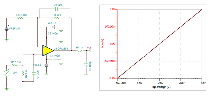
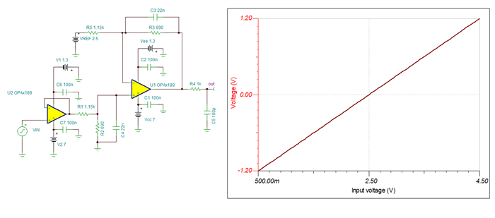
    A difference amplifier with a gain of 0.6-V/V can be used, such as below.

    If the sensor can drive the 1.690kΩ difference amplifier input impedance directly, the OPA388 powered with Vs+ = +2.5V and -2.5V supplies will work.  The circuit requires low drift, high precision resistors and a low drift, high precision reference of +2.5V. producing total output noise of about 12uVRMS.  See below. 

    If the sensor requires a high input impedance, or can not drive the voltage divider directly, a low drift, low noise dual op-amp OPA2189, powered with bipolar supplies, Vs+ > +7V, Vs- < -1.7V can work on a similar circuit.  The circuit requires low drift, high precision resistors and a low drift, high precision reference of +2.5V. producing even lower noise, a total output noise of around ~6.38uVRMS.  See below. 

    Thank you and Best Regards,

    Luis

  • HI Kaveh, 

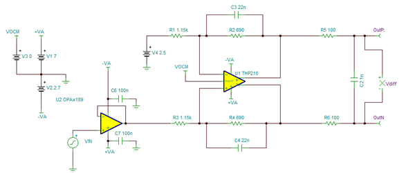
    Since the ADS131M08 also supports fully-differential inputs, the single OPA189 can be used as a buffer and a fully-differential THP210 could be used to convert the single-ended signal to fully differential. For this circuit, connect the VOCM pin of the THP210 to GND.  The noise performance is similar, just slightly lower at around ~5uVRMS.  The offset drift of the THP210 is very low for a fully differential amplifier.   The offset drift of the THP210 just a little higher compared to the previous zero-drift amplifier suggestions on the posts above, but still a low drift solution.  The circuit requires low drift, high precision resistors and a low drift, high precision reference of +2.5V.  The devices will require bipolar supplies.

    Thank you and Regards,

    Luis

  • Great. I dont have a 2.5V supply level in my design. I only have 5V and 3.3V. Is there a chip that can generate +2.5V and -2.5V reference voltages from a single positive 5V or 3.3V that I have available for the design you are proposing. 

    Thanks

  • HI Kaveh,

    In an application that does not have a negative supply, the easiest method to drive the ADC is using a fully differential amplifier (FDA), centering the fully differential signal (±1.2V) at a common-mode voltage of AVDD/2= +1.65V. I originally thought you were actually requesting a level translator to shift the absolute voltage to -1.2V to 1.2V range, ie, to an absolute voltage below ground.

    The ADS131M08 incorporates differential inputs, and offers flexibility with the input common-mode voltage. The device allows absolute voltages anywhere in the range from -1.3 to AVDD (+3.3V), where the fully differential ADC inputs converts the difference (AINP- AINN). Although the device supports absolute negative voltages (voltages below GND), the differential input ADC is flexible and does not necessarily require the input signal shifted to an absolute voltage below ground. 

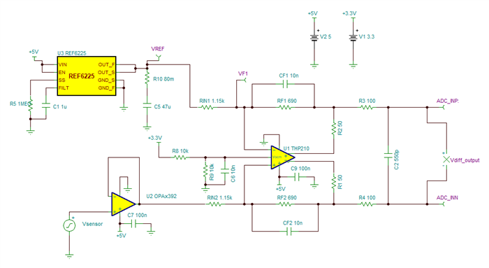
    The THP210 is a FDA that can be used to convert the sensor single-ended signal (+0.5V to +4.5), to a fully-differential signal ±1.2V, where the differential voltage signal is centered at AVDD/2= +1.65V common-mode voltage. 

    Hence, the circuit does not require a negative supply.  Please note, you will still require a high precision +2.5V, low noise, low drift reference capable of driving the input impedance of the fully-differential amplifier.  The REF6225 2.5V low noise, low drift, voltage reference will work well in this case powered with the +5V supply.  If your sensor requires high impedance, use a +5V precision, low drift amplifier such as OPA392 to buffer the sensor prior the FDA. 

    The THP210 is powered with the +5V supply, where the RIN (1.15kΩ) and RF (690Ω) FDA gain resistors need to be low drift, precision (or matched drift) resistors. The VOCM pin voltage needs to be set to a voltage AVDD/2= 1.65V, using an external resistor divider connected to +3.3V supply; nevertheless, the VOCM voltage divider resistors do not have to be high precision. 

    The noise of the overall circuit is about 6uVRMS.  I adjusted the R-C-R filter filter to drive the ADC for stability/settling purposes.  The feedback capacitors (CF) can be adjusted per your sensor signal bandwidth requirements.  As shown, with CF=10nF, the f(-3dB) bandwidth is around ~23kHz. Use C0G/NPO capacitors at the feedback (CF) and ADC input RCR filter

    See one possible circuit below, powered with +5V and +3.3V supplies.

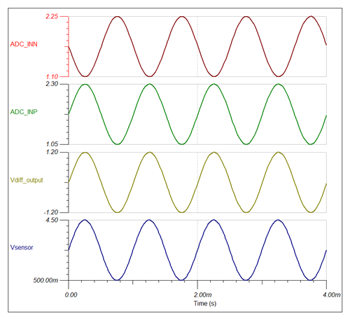
    See transient simulation below, with the fully-differential signal ADC INP-INN is ±1.2V amplitude, centered at +1.65V DC

    Thank you and Regards,

    Luis Chioye  

    TINA simulation file

       THP210_ADS131M08_forum1.TSC

  • Thank you. Can you please explain what you mean by "I adjusted the R-C-R filter to drive the ADC for stability/settling purposes". I am wondering why you have chosen 100ohm/560pF RCR filter at the input of the ADC. Because in ADS131M08 datasheet the recommended RCR values are 50ohms/4.7nF.

  • Hi Mohammed,

    There is a level of flexibility.  The ADS131M08 is a Delta-Sigma ADC, and this device, when compared to other architecture ADCs such as SARs, offers relatively high input impedance as described on the datasheet, and does not have a very strict R-C-R filter requirement from the ADC drive perspective.

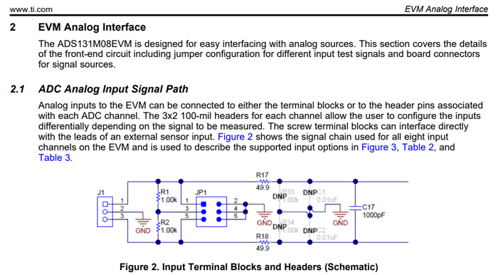
    For example, the ADS131M08 datasheet  Figure 9.1 of the ADS131M08 datasheet shows an R-C-R filter of 1k-10nF-1k with a corner at 7.8kHz , where the datasheet recommends this low frequency filter for anti-aliasing filtering purposes. The design guide, for a 3-phase CT Meter reference, uses  1k-6.8nF-1k. However, the ADS131M08EVM user guide (below) shows an higher frequency ADC input filter with 49.9Ω - 1nF - 49.9Ω  with a corner around ~1.6MHz.

    See below:

    As we discussed, on the THP210 circuit example on the previous post, the dominant filter pole for anti-aliasing purposes perspective is set by the feedback components (RF= 690-Ohm, CF=10nF) around ~23kHz, but as I have mentioned, the feedback capacitor can be adjusted per the application bandwidth requirement.  For example, Increasing the feedback capacitor can reduce the circuit bandwidth, if you are primarily interested in low frequency signals. The filter at the THP210 output 100Ω - 550pF - 100Ω has been simulated for amplifier stability (together with the feedback and other components), offering 56-degrees of phase margin. The output filter, has a very similar corner of 1.45MHz as the one featured on the ADS131M08EVM.

    The circuit can be modified with the suggested filter on your post, the THP210 with the 50Ω - 4.7nF - 50Ω (677kHz pole) filter at the output, and after adjusting the feedback components for example to (RF= 690-Ohm, CF=1nF) is stable as well, offering about ~50-degrees of phase-margin, and this will set your overall corner frequency at around ~176kHz.

    The queries above does not discuss the application bandwidth requirement, so I provided an example. You could certainly adjust the feedback and output filter circuit components depending on the bandwidth, settling requirements while ensuring the amplifier remains stable. What figure on the ADS131M08 datasheet recommends the 50ohms/4.7nF? and what bandwidth do you require?

    Thank you and Regards,

    Luis


  • Luis, what is the reason you chose 50 ohms for R1 and R2 in the output of the differential amplifier THP210?

  • HI Kaveh,

    In some cases, the resistors connected at the outputs of the FDA, inside the feedback loop of the THP210, of a few ~10s of ohms, can be helpful improving the loop gain response and increasing phase margin while driving the R-C-R filter at the THP210 output.

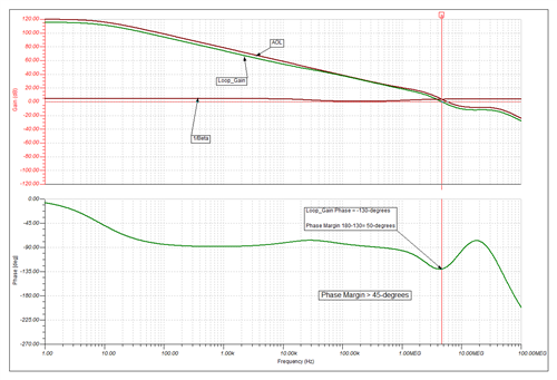
    A separate open-loop AC simulation analysis confirms the circuit has about ~50-degrees of phase margin exceeding the ~45-degrees phase margin (conservative) guideline. This circuit is stable. Using these resistors inside the feedback can help smooth the loop-gain response removing abrupt changes in the phase-loop response while driving RC filters or capacitive loads.  In this case, simulating the circuit with the filter at the THP210 output (100Ω - 550pF - 100Ω), the 50-ohm resistors inside the feedback loop improve the phase-margin slightly, from ~45-degrees to ~50 degrees.  In this case, the ~50-ohm resistors are not absolutely required, but they are improving phase margin by 5-degrees, and it may be a good idea to have footprints for these on the PCB for flexibility.    

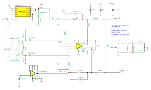
    Below is a circuit used for verification of stability performing the open-loop, small-signal loop-gain test on SPICE simulation.  The large inductors (L1, L2) are used in the simulation to open the feedback loop for AC frequencies.  The large capacitors (C1_, C2_) are used in the simulation to inject an AC test signal source.

    The user needs to monitor the phase-shift or the phase change to the frequency where Aol*Beta = 0-dB.  Depending on the circuit configuration, and how the feedback loop is open and/or the test source is injected/applied, the SPICE simulation may produce a different starting phase, in some cases different than 0° degrees at low frequencies (frequencies close to DC).

    The phase margin is determined by monitoring the loop gain crossover when |AOL*Beta| =1 or 0-dB.  To calculate the phase margin, we monitor the change in the Loop-Gain phase from low frequency (close to DC) to the crossover frequency.  In this TINA simulation, when opening the feedback loop and measuring the Loop-Gain phase, the phase starts at low frequencies close to 0°-degrees. The loop-gain phase at fcl (frequency where loop gain is 0-dB) is -130°degrees. The phase shift or phase change from low frequency to fcl is -130º degrees. The phase margin is calculated as the difference from ±180°phase shift, or 180°-130° = 50° phase margin.  

    AC Open-Loop Analysis File: 

    THP210_ADS131M08_forum_stability_12-01.TSC

    For more detailed information on the procedure for this stability analysis, please review the below TI  video for tutorials

    Thank you and Best Regards,

    Luis

    Stability analysis is quite an extensive topic to discuss in a single forum post, and there are several methods to analyze stability.  You can learn some basics about amplifier stability on the following resources:

    https://e2e.ti.com/support/amplifiers-group/amplifiers/f/amplifiers-forum/1048137/faq-documents-about-op-amp-stability

    Fully-Differential Amplifier Stability:

    FDA stability and simulating phase margin

    Also helpful, op-amp stability: