This thread has been locked.

If you have a related question, please click the "Ask a related question" button in the top right corner. The newly created question will be automatically linked to this question.

INA220: Measurement error between INA220A and INA220B

Part Number: INA220
Other Parts Discussed in Thread: INA232, INA234

Hello,

My customer wants to do voltage sensing using INA220.

If the device setting is 0~16V and the actual input voltage is 0.1381V, can you tell me how much the measurement error difference will occur between INA220A and INA220B?

They say that it is not easy to predict measurement error from data sheets alone.

Thank you.

JH

  • Hello Valued Engineer,

    It does not seem like there would be any difference in bus voltage measurement error between A and B versions. This answer feels simplistic, but it is valid.

    Sincerely,

    Peter

  • Hello Peter,

    Thanks for your reply.

    I'm sorry, but there was a mistake in explaining the customer's inquiry.

    What my customer wants to know is the voltage error for low input voltages for the INA220A and INA220B.

    They are concerned that if the input voltage to VBUS is 0.1381, the detection error will be too large because the input voltage level is too low.

    Could you please tell us what the voltage error will be for the 0.1381 input voltage?

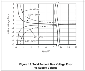
    It is not easy to estimate from the picture below.

    Regards,

    JH

  • Hey JH,

    No worries, I should have elaborated further. I understand it is hard to see what it would be.

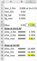
    There is not direct specification for VBUS offset, which will be the dominant source of error at VBUS=0.1381V. I have back calculated the error with offset specifications of 8mV and 20mV for 3.3V and 5V supply voltages and 0.10% gain error. Based upon these curves, the error at 0.1381V VBUS will be 5.81% for 3.3V supply.

    I used Figure 5 to approximate typical VBUS offset values.

    Hope this helps.

    Best,

    Peter

    INA220_VbusError.xlsx

  • Hi Peter,

    The customer changed only the INA220 on one board and checked the 0.1387V voltage input above.

    The test results are as follows.


    VBUS value (V)

    BUS Voltage Register (BRNG=0)

    Calculation (bit [14..3] * 0.004) (V)

    Tolerance

    INA220 #1

    0.1387

    14a

    0.164

    18.2%

    INA220 #2

    0.1387

    132

    0.152

    9.6%

    A higher error occurred than the expected 5.81% error.

    What are some factors that may cause actual measurement results to have higher-than-expected errors?

    The above test only changed the device under the same external conditions. What causes the error to vary greatly depending on the INA220 device even though the external conditions are the same?

    Thanks,

    JH

  • Hey JH,

    What is the supply voltage?

    What is the full-scale setting for VBUS register?

    May I get a basic schematic and test setup? 

    Any layout information about system, load, instrument grounding will also be helpful.

    As you can see in the tabulated error I sent above, the VS level can dramatically shift the VBUS offset up to 14.49% with a Vos_bus = 20mV. 

    Sincerely,

    Peter

  • Hi Peter,

    Below are the customer responses.

    1. Supply voltage = 3.3V
    2. VBUS register : full-scale
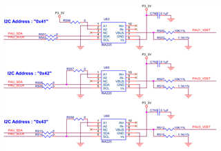
    3. Basic schematic :  - Three INA220s are used within one board, and PAUx_VDETs are connected to different external modules (The external module is the same design product).- As a result of checking multiple products, the error occurrence points are not constant.
      - If they replace INA220 in the same location, the detect level will change(Therefore, deviations occur depending on the device, regardless of the board environment).

    Is VBUS offset a characteristic that varies depending on the device? Or is it also related to the external environment?
    (For example, 3.3V power characteristics (ripple, etc.), ripple characteristics of VDET signal, etc.)

    Thanks,

    JH

  • Hey JH,

    VBUS offset can definitely change with VS as seen in the datasheet plot. Also keep in mind you are adding -0.31% gain error with the 10k/1k resistor divider at input pin. 0.31% = 1 - Reff/(320k+Reff) where Reff = 10k||1k and 320kΩ is the input impedance of VBUS pin. The error can easily reach up to 0.35% if the internal 320k varies by -10% (it probably could go up to +/-20% over process variation).

    I would double check the accuracy of your voltmeter and make sure that it is probing at VBUS pin and GND pins of INA220 for most accurate reading to compare against the digital measurement.

    If you see the offset follow the devices when swapping device locations then you know if must be something with the device.

    Aside from all of this, this device does not have a final test screened VBUS offset voltage, nor does it have a bus offset PSRR (power supply rejection ratio) specification. Thus, the VBUS offset is not tightly controlled and it is possible there is a 25.1mV offset = (18.2%)/0.1381V. Additionally, VBUS offset could be proportionally of inversely related to VS. 

    The only screened VBUS error specification is the error at VBUS=12V, but at this point offset error will be negated and error will be dominated by gain error.

    If high accuracy at low VBUS is required, you may need to consider switching to a power monitor that this specification such as the INA234 or INA232.

    https://www.ti.com/amplifier-circuit/current-sense/digital-power-monitors/products.html 

    Sincerely,

    Peter

  • Hi Peter,

    Thanks for your help.

    The customer has additional questions as below.

    Thus, the VBUS offset is not tightly controlled and it is possible there is a 25.1mV offset = (18.2%)/0.1381V. Additionally, VBUS offset could be proportionally of inversely related to VS. 

    Q1. Could you please tell us where they can find the source of the 25.1mV offset voltage?

    Q2. Does 'it is possible there is a 25.1mV offset' above mean that the offset voltage can change up to 25.1mV momentarily? Or is it that some devices may have an offset voltage of 25.1mV?

    BR,

    JH

  • Hey JH,

    Q1. The source of the 25.1mV offset is the inherent to the INA220 and instrument tolerance.

    Q2. It just means that in a population of INA220 there could be some device that have offsets of 25.1 mV. Offsets do no change unless another condition is changing such as Vs, Vbus or temperature.

    Sincerely,

    Peter