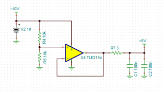
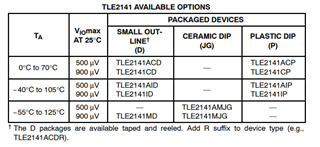
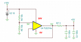
This thread has been locked.
If you have a related question, please click the "Ask a related question" button in the top right corner. The newly created question will be automatically linked to this question.
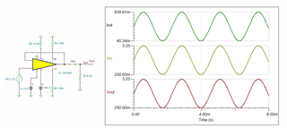
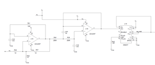
We are using this device as an output buffer in a circuit that creates a 5VAC signal at 440 Hz. The equipment it feeds into draws about 800mA from the OPA567. The op amp current limit is limited to 1.1 A in the circuit. The TI simulator software indicates that the device would have to operate at a supply voltage of +8.8 VDC to accurately create the 5VAC signal at 440 Hz. This is a single supply circuit so the other end of the supply is ground. At first we hesitated to power it at 8.8 VDC due to your data sheet's max rating of 7.5V, but we were too far into this design to start over with a different device without significant data to indicate the risks. (This situation resulted from design criteria that changed recently.) We tested our circuit with the OPA567 at 8.8 VDC and used a FLIR camera to record the temperature of the package top. It levels off at 220 degrees F. We ran it for several hours like that in an environment of 160 degrees F with no obvious impact. We do not have the Tflag pin connected to anything in the circuit. We want to best understand what you can tell us about this so we can evaluate impact of continuing.
Hi Lyle,
I'm not sure what you mean by "The TI simulator software indicates that the device would have to operate at a supply voltage of +8.8 VDC to accurately create the 5VAC signal at 440 Hz." What software are you using? Using TINA-TI, I can simulate the circuit to successfully produce a 5Vppk output at 440Hz with a 1.1A current-limit and ~800mA peak output current.
Is your 800mA current load RMS or peak? If it is 800mA RMS, it is possible that your 1.1mA current-limit is set slightly too low to source the peak current into the load.
According to the datasheet, there is no limitation in output swing or full-power bandwidth that would prevent the OPA567 from producing the desired output while operating on a 5.5V supply. Operating on 8.8V supply is not necessary and certainly not recommended as this can damage the device and/or effect long-term reliability by operating outside of the absolute maximum ratings.
Regards,
Zach
Apologies, I got several details wrong. The oscillator op amp ahead of the OPA567 creates the 5VAC signal which is RMS, and that signal feeds into, and out of the OPA567. It's 400 Hz not 440. The oscillator op amp is made by a different manufacturer which can handle the 8.8V and the software we used to tune in the AC signal was LTspice. Our power rails, +V and GND, are connected to both the oscillator amp and the OPA567, so when we raised the power level to tune in the oscillator, the power to the OPA567 raised too. Now the question changes. Are we seeing the OPA567 get so hot because of the 8.8V power, or because it is sourcing 800mA? You mentioned the current limit so I wonder if the OPA567 is heating up so much because of that?
Hi Lyle,
Can you provide a schematic of the proposed circuit? What is the exact voltage range of the oscillator signal? For example, 0.2V to 7.27V or 1V to 8.07V. We will need to consider the exact minimum and maximum voltage to ensure the input common-mode range and output voltage swing of the amplifier can accommodate the signal.
The OPA567 is specified up to a power supply of 5.5V and therefore it cannot accommodate an input/output signal that is wider than the supply. Operating at 8.8V is a violation of the abs max and is not a valid operating condition. It is possible that this violation of the power supply range could contribute to increased internal power dissipation which is heating up the op amp as you noticed. Regardless, we will need to find a solution that operates within the power supply requirements.
The main concern is ensuring there is enough headroom to the supply rails to accommodate the output swing. As power amplifiers are expected to supply high current, the output swing is often limited to some volts from either rail. Is the oscillator op amp required to operate on exactly 8.8V? or can the supply be increased to say 10V or 12V?
Another option if you want to avoid qualifying another device, is to use a power-supply "bootstrapping" technique using two additional OPA567 to modulate the power supplies in response to the output swing. The technique is detailed in the OPA462 application note as well as a THS3491 reference design, both linked below. The additional op amps (U2 and U3) will shift the positive and negative supply voltage of U1 up and down to allow the output to swing wider than the maximum single supply voltage, without violating the abs max. I simulated this in TINA-TI below, notice that Vcc and Vee are modulating with the signal voltage, while the total supply voltage (Vcc-Vee) remains fixed at 5V.
For a detailed analysis of this technique, please refer to the documents linked below.
Techniques for Extending the Usable Power Supply Range of the OPA462 High-Voltage Op Amp
Design Guide: Bootstrap High-Output Voltage-Extension Reference Design
Regards,
Zach
While I work to gain approval to send you the circuit, I’ll give you more information. The output signal is a sine wave with peaks at 7.0 and 0.7 volts. The oscillator op amp and OPA567 both have the same power rails, but we could change that and power the OPA567 or it’s replacement with a different single supply power that is 8.8V or less. We could use a regulator or a voltage divider. Our major limitations are board space and what parts are available through the spotty supply chain. The board space we have to handle any replacement to the OPA567 is a square approximately 1.3 inches by 0.3 inches. Also, we connected equipment to the OPA567 output that drew only 100 mA and the temperature of the OPA567 package never raised above 100 degrees F. But it was still being powered at 8.8V.
Hi Lyle,
I can't provide much guidance on the thermal operation of OPA567 when powered on 8.8V, as this is outside the operating range of the device and a violation of the absolute maximum conditions. Any operation at this power supply level is neither specified nor characterized and will likely result in damage or effect long-term reliability.
The oscillator op amp and OPA567 both have the same power rails, but we could change that and power the OPA567 or it’s replacement with a different single supply power that is 8.8V or less.
Why is the single-supply limited to 8.8V? I see that the oscillator amp can be powered as high as 50V. If the power supply can be increased to say 10V, I believe we can find a power amplifier that will accommodate your signal range.
The OPA564 is specified to operate on supplies between 7V and 24V and can output up to 1.5A. It has an input common-mode limitation of 3V from the positive rail, so it will require a power supply of 10V to accommodate the 7V max input signal.
The output voltage swing is dependent on the current being sourced. For a 10V supply there will be plenty of headroom to supply the peak 1.2A @7V. The output can swing very close to the rail for relatively smaller load currents as shown in the figure below. Is the load referenced to ground? Assuming a purely resistive 6.25Ω load referenced to ground, the 700mV minimum output voltage corresponds to 112mA, which appears to be low enough to allow the amp to swing within 700mV of the negative rail. Of course, you will need to verify this for your actual load.
I believe this 10V OPA564 solution or the bootstrapped 3-amp OPA567 solution are the best options. Operating OPA567 on 8.8V is not a valid option for a reliable design.
Regards,
Zach
The oscillator circuit is designed to be powered by the input voltage. 8.8V input & power rail gives the correct 5VAC signal. There are 2 problems I see with the OPA564. 1) Our circuit cannot sequence the power supplies as required in fig. 36 on page 14 of the OPA564 data sheet. 2) The temperature requirement for our application is -46 degrees C. The low temperature operating limit of the OPA564 is -40 degrees C. Sorry I neglected to mention that earlier. Our high temperature requirement is +71 degrees C, so that’s not a problem. It looks like we could modify the oscillator circuit to power it using +10V and use a voltage divider to make its input 8.8V which allows the oscillator to output the same 5VAC signal. Now I have a few questions on the bootstrapped circuit you provided above. 1) Why are the Tflag and Iflag inputs tied to +5V? 2) Why is the Vin set to 4.5V? 3) Is R3 present to create a load when no load is present, or is it present only to make the simulation work? 4) We would be creating the +5V supply from a voltage divider on the +10V supply. What range of resistors (e.g., 1K, 10K, 100K) is needed on the voltage divider for U2 & U3 to draw the current they need for this design?
Hi Lyle,
Thanks for the additional information. I see that due to the temperature range requirements you want a device that is specified to -55C. One thing to consider is that if you are dissipating power in the device, the junction temperature will likely be much higher than -40C even if the ambient temperature is at -46C. For this reason I wouldn't rule out the OPA564. I'm sure the digital power supply sequencing solution will be relatively trivial compared to the bootstrapping power supply alternative discussed below.
1.) Why are the Tflag and Iflag inputs tied to +5V?
The TFlag and IFlag are CMOS outputs that switch between V+ and V- to indicate the flag condition. For all 3 amplifiers in the simulation, I used a 100kΩ pull-down resistor connected to the respective V- voltage of each amplifier. This was simply done to indicate that because each of these amplifiers have different power supply voltages, each of these output flags are referenced to a different voltage. If anything in the circuit is connected to these flags, such as a digital I/O, you will need to ensure that any connected voltages are compliant with the abs max ratings.
If these flags are not used or monitored in the circuit, you may leave them floating to save space on the board.
2.) Why is the Vin set to 4.5V?
I set the DC value for Vin centered around 4.5V as the assumed mid-point of the input signal. For a signal from 0.7-7V, the mid-point is 3.85V.
3.) Is R3 present to create a load when no load is present, or is it present only to make the simulation work?
R3 simulates the load you are driving. The value 6.25Ω is derived from your 5V RMS output voltage divided by the 800mA RMS output current. What is the load you are attempting to drive? Can you provide the load impedance? Is the load referenced to ground (0V) or some other voltage?
4.) We would be creating the +5V supply from a voltage divider on the +10V supply. What range of resistors (e.g., 1K, 10K, 100K) is needed on the voltage divider for U2 & U3 to draw the current they need for this design?
Typically, a high output-current power source cannot be derived directly from a voltage divider and will require an additional high output-current buffer to supply the desired current. For example, the peak 1.2A across a 1kΩ resistor would result in 1200V which is not practical.
Assuming the load is referenced to ground, in this circuit the amplifier is always sourcing current which means that the output current will be supplied by the V+ of U2 which is the 10V supply. In the case that the amplifier is required to sink current, the current will be sunk through the V- supply of U3 which is ground. The 5V supply is only required to source/sink the quiescent current or U2 and U3 which is 11mA max. This can be achieved with a voltage divider and a simple op-amp buffer that only needs to output up to 11mA.
I updated the schematic with the current limit set to 1.2A, the TFlag and IFlag pins floating and the input/output corrected to 0.7V-7V @400Hz.
OPA567_0.7_to_7V_Bootstrapped.TSC
Regards,
Zach
On the OPA564, our customer has the final approval of all of this and despite the reality of the device power dissipation elevating the temperature, they will see the temperature limit as noncompliance and strike it down. We are leaning toward the bootstrapping design now. For the Tflag & Iflag outputs, I thought maybe you have them connected to +5V for the simulation software but wanted to be sure. Regarding R3, I expected that presented a load to the circuit. Your R3 load will be sufficient for this investigation. Also, our load is referenced to ground. On the voltage divider for the +5V supply, we can use another OPA567 for that, per your recommendation. That results in adding 3 more OPA567s and several supporting components to implement this design. We may be able to accomplish that with the space we have. It’s more than the 1.3 x 0.3 inches, but we might be able to recover some space in other spots on the board. For that reason, I’m going to call this issue resolved. Thanks very much for the help and the quick responses to my posts.
Hi Lyle,
I'm glad to hear that the bootstrapping circuit is acceptable for your design, hopefully your customer accepts the modifications.
One additional comment, you will not be able to use a fourth OPA567 to buffer the 5V supply, as the selected op-amp must be powered on your 10V supply. You will need to select an amplifier that can be powered on 10V, supply at least 11mA, and operate down to -55C per your customer requirements. Most TI devices that operate at -55C feature the "M" or "-EP" suffix. I recommend the TLE2141M-D to drive the 5V supply as shown below.
A 3Ω isolation resistor provides sufficient phase margin for closed-loop stability when driving the two 100nF decoupling capacitors that are typically placed locally at the op-amp power supply pins.
https://www.ti.com/product/TLE2141M-D
See the updated schematic below showing the TLE2141M in your bootstrap circuit.
OPA567_Bootstrapped_TLE2141_5V.TSC
Regards,
Zach
Yes, I missed that detail. I downloaded the data sheet on the TLE2141 device and I'm confused. Your web site shows the TLE2141M-D and how many are in distributor stock, under a part number without the dash. But the data sheet doesn't show any M-D versions, just MFK or MJG. How am I to interpret that for what specs the D version has differently from the others, or know what part number variations to order?
Hi Lyle,
My apologies, the link I sent you leads to an older version of the datasheet. I'll reach out to the web team to get that fixed.
The updated (Rev. D) version of the datasheet can be found under the main TLE2141 product page: https://www.ti.com/product/TLE2141
I've also linked it here: https://www.ti.com/lit/ds/symlink/tle2141.pdf
Rev. D of the datasheet includes the "M" device in the D package. The updated orderable is "TLE2141MDR" for the tape and reel option.
The "G4" suffixes from the other product page are an older naming convention that TI is in the process of phasing out. Apologies for the confusion.
Please let me know if you have any more questions.
Regards,
Zach
Glad to get the correction. I looked over the new data sheet and it looks like what I expected. I wondered why the data sheet didn't include the typical information of the variants. Next, after reviewing the +5V buffer configuration again I think we need to compensate for the output not being able to swing from rail to rail. The spec shows typically a 4.1V output limitation on a 5V powered device. Do we need to change the divider to input 6V to the buffer so it can output 5V? I also had a collogue raise a question I had to make assumptions about to answer, so let's clear that up too. The question is - on the bootstrapped circuit the resistors on the Vout output create a voltage divider from +10V that would make Vout become +5V. They were concerned that a 5V signal would interfere or add to the output. I told them that Vout likely becomes +5V at the instant power is applied but the op amps, being active devices, would control the voltages & currents to change the voltages across that "divider" to create the AC waveform shown in your simulation. Please confirm or correct my explanation.
Hi Lyle,
The +5V buffer is powered by Vcc=10V and Vee = 0V and the 5V input voltage is generated from a voltage divider on the 10V supply. The +5V buffer amplifier does not need to be rail-to-rail in this case because both the input voltage and output voltage are at mid-supply, that is Vcc-5V = 5V = Vee + 5V. The TLE2141M has no issue swing 5V from either rail on a 10V supply.
I would like to change R3 to about 6K so when we add the real load the device isn't pulling double the current, but would still be present to facilitate a light load for troubleshooting purposes. Is this sound reasoning, or not?
This is very reasonable. The 6.25Ω resistor is simply included in the simulation to simulate the load and should not be included in the actual schematic as this would double the load as you mentioned. As you suggest, placing a 6kΩ load resistor provides a reasonable load to ground that can be adjusted to help with troubleshooting.
The question is - on the bootstrapped circuit the resistors on the Vout output create a voltage divider from +10V that would make Vout become +5V.They were concerned that a 5V signal would interfere or add to the output. I told them that Vout likely becomes +5V at the instant power is applied but the op amps, being active devices, would control the voltages & currents to change the voltages across that "divider" to create the AC waveform shown in your simulation.
I think I understand the confusion. You are mostly correct in your assessment. U1 is an active device that is directly driving the Vout node and therefore the Vout voltage is determined by the operation of U1. If you are considering only the four 100kΩ resistors, you are correct that these would weakly pull the Vout node to 5V (similar to a digital pull-up resistor), however the output drive of U1 will easily overcome this and drive the node to the correct AC waveform.
In the case that U1 is INACTIVE while the power supplies are ON (this can be done with the enable pin function), the output voltage will not reach 5V as the load resistance is also pulling the output to 0V. A 6Ω load resistor to ground easily overcomes the 100kΩ resistors and the output is very close to 0V. A 6kΩ resistor to ground is still much stronger than the 100kΩ resistors and the output will sit a few 100mV above ground as determined by the voltage divider equations.
I hope this clears things up.
Regards,
Zach
For the 5V supply - I seem to keep forgetting +10V is powering the TLE2141MD. I've got it now. For the 6 ohm being replaced by 6K, thanks, I'll do that. And, thanks for the detail on Vout. I'll post this and then mark it as resolved.