This thread has been locked.

If you have a related question, please click the "Ask a related question" button in the top right corner. The newly created question will be automatically linked to this question.

OPA567: OPA567

Part Number: OPA567

Hello, ART

OPA567: Design review - Amplifiers forum - Amplifiers - TI E2E support forums

3. Output swing limit - the output swing limit is 0.2V for light load and good linear response, and 0.3V under heavy load.  So, technically, you are close to this limit and/or violating this limit for low current levels.  You can confirm if this is a problem or not.  The diode voltage jumps up fairly rapidly when even low levels of currents are applied so as long as the diode drop is 0.3V or greater you should be ok.

=> So, technically, you are close to this limit and/or violating this limit for low current levels.
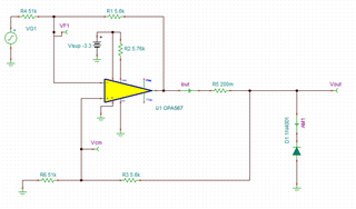
Q1. How can the issues related to the low current level be addressed in the above circuit?

      Would using dual power supplies (+3.3V/-3.3V) resolve operational issues at low current levels?

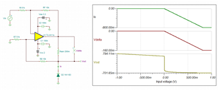
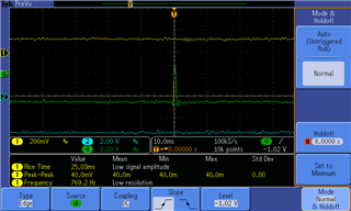
     When using an input voltage around 0~0.2V, a pulse similar to the one shown in the diagram occurs at the Vcm of OPA567.

     This pulse continues to increase, causing the OPA567 to malfunction.
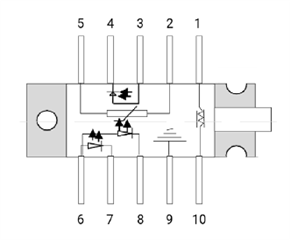
Q2. Is there an alternative circuit configuration to use the Laser Diode type shown below, aside from the one depicted above?
Thank you.

  • Hi Joung,

    Q1. How can the issues related to the low current level be addressed in the above circuit?

    OPA567 is unable to provide accurate current source below ±0.2A

    Q2. Is there an alternative circuit configuration to use the Laser Diode type shown below, aside from the one depicted above?

    You may use TLV411X part, which is able to source up to 300mA or slightly more.  

    TLV4111x current source.TSC

    What are the application's current range and how accurate is the current source per the requirement? What is your voltage transient step? 

    Since this is low voltage current source application, we may adapter current booster design from Howland Current application. Your available supply voltage rails are a bit low, otherwise we have other options. 

    https://www.ti.com/lit/an/snoaa46/snoaa46.pdf?ts=1707859532698&ref_url=https%253A%252F%252Fwww.google.com%252F\

    https://www.ti.com/lit/ug/slau502/slau502.pdf?ts=1707869238054&ref_url=https%253A%252F%252Fwww.google.com%252F

    If you have other questions, please let me know. 

    Best,

    Raymond

  • Hello, Raymond

    First of all, thank you for your response.

    I have an additional question.

    The circuit, composed of OPA567, is experiencing sudden failure to operate during driving.

    When checking the OPA567 pins at this time, they are as follows:

    ( Input voltage : 200mV )

    1. Iset(pin 6) : -3.3V

    2. VO(pin2,3) : 0V

    3. V+( pin1,12) : 0V

    4. V-(pin 5,4) : -3.3V

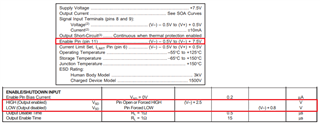
    5. Enable(pin 11) : 0V

    6. -IN(pin 8) : 0V

    7. +IN(pin 9) : 0V

    Please share your opinion on what events may lead to the occurrence of this phenomenon

    Thank you.

  • Hi Joung,

    I do not have enough information to suggest what is the root cause that damaged the OPA567. Please provide me with additional test details. 

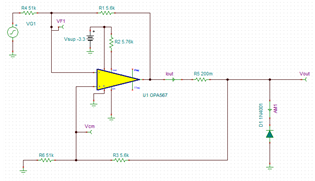
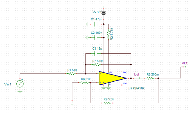
    Are we talking about the Howland Current OPA567 shown in the circuit below? In the difference amplifier, the input is -200mV (0-200mV) and the output current should be -200mV*0.196V/V/0.2 Ω = -196 mA. Does your laser diode have long leads with inductive load? Are you input the pulsed 200mV at the input? How is OPA567's heatsink connected to? Anyway, I need these details. Please let me know. 

    Best,

    Raymond

  • Hello, Raymond

    I am using a Dual Laser Diode.

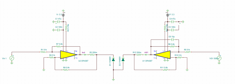
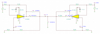
    So, I have a structure similar to the diagram below.

    The input voltage range is 0V to 2V, and the desired output current range is 0A to 1A.

    I expect the calculated value of -(Vin/0.2Ω)*(51k/5.6k) and The input is of sine type, not pulse type.

    Question 1.

    In the configuration shown above, when the Dual LD is removed and the voltage at VF1 is checked, some samples exhibit a voltage close to 0V.

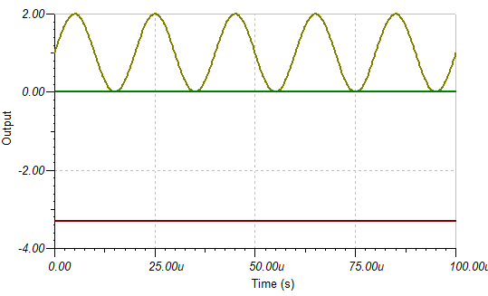
    Why is VF1 not measuring -3.3V as shown in the simulation above?

    Best,

    BongJo

  • Hi BongJo,

    -(Vin/0.2Ω)*(51k/5.6k)

    You had a typo. The circuit gain is 10k/51k or close to 0.196. So the negative input voltage delta translates into the -Iout in current at the output. 

    In the configuration shown above, when the Dual LD is removed and the voltage at VF1 is checked, some samples exhibit a voltage close to 0V.

    Is the OPA567 working? Is it damaged?

    Please use the current meter to measure the output current, if you removed the dual LDs. Typical DMM has input impedance of 10MΩ to 10s GΩ. If you connect a DMM as the current source at the output. My guess is that the OPA567 may hit the rail voltage or in a protection mode. In any case, the OPA567 is not operating in linear mode at this point with DMM measurement.  Please try it with current meter and let me know. 

    Best,

    Raymond

  • Hello, Raymond

    Raymond said:

    Is the OPA567 working? Is it damaged?

    => It is working. However, I cannot be certain whether these anomalies are causing cumulative damage to the OPA567.

    Please try it with current meter and let me know. 

    The measurement points below are between VF1 and GND, and were measured using a DMM

    => 1) VF1 (-3.3V) : 0A

         2) VF1(0V) : 0.36uA

         3) VF1(0V) :-0.03uA

    Are these aspects causing damage to the OPA567?

    Best,

    BongJo

  • Hi Bongjo,

    OPA567 requires to source/sink ±200mA current. I was wondering if this is what you are observing. 

    Please supply the input voltage above 0.2V when you make the above measurement. Please tell me the input voltage signals when you measure the static measurement. I would like to see the input and output responses together. I am unable to interrupt data without knowing the input voltages.  

    If you have other questions, please let me know. 

    Best,

    Raymond