Other Parts Discussed in Thread: THS7530, LMH2832, OPA855, OPA818
Hello TI experts!
We are considering using the THS7530-Q1 in our application and have a few questions that I hope you can help clarify.
Question 1: I do not see a SPICE model listed on the TI website.
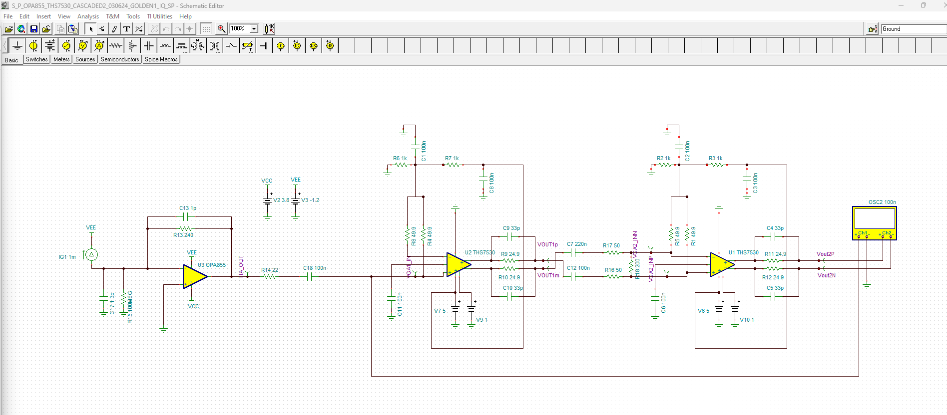
- Does a PSPICE model exist so I can model the behavior for our intended purposes in TINA?
Question 2: In the datasheet on page 1, under Description it states: "The THS7530-Q1 device is a DC-coupled, wide, bandwidth amplifier".
- We would like to use this VGA in a cascaded (two-stage) setup in order to boost the overall gain range to suit our needs. At the same time our application requires the ability to allow 0dB gain so I'm planning on attenuating the signal such that we have 0-34.9dB gain range for each stage as opposed to 11.6 to 46.5dB. In our application we would use the first stage with single ended input, differential output and the second stage as differential input and differential output. Will this device support such a cascaded setup? The input signal varies between ~1MHz - 75MHz over an anticipated ~56dB overall gain envelope.
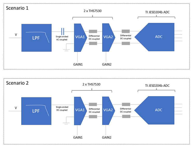
- We would like to be able to use the first stage in a DC-coupled setup (scenario 1) and also another instance where we use the first stage in an AC-coupled setup (scenario 2).
The output of the first and second stage would be differential and DC-coupled as shown in the image below.
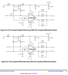
Section 9.1 Application Information of the datasheet suggests that this *can* be accomplished. However I believe there may be an error in Figure 21 "DC-coupled single-ended input with DC-coupled differential output". The figure shows an AC-coupling capacitor at the single-ended input. I'm assuming that the description should state: "AC-coupled single-ended input...."?
I just to confirm that the two scenarios shown in the image below are valid applications for this device.
Thank you for your feedback,
Peter


