This thread has been locked.

If you have a related question, please click the "Ask a related question" button in the top right corner. The newly created question will be automatically linked to this question.

OPA548: OPA548

Part Number: OPA548
Other Parts Discussed in Thread: , OPA547, OPA593

Hello,

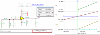
A diagram of a non-inverting amplifier can be found below.
Power source (single supply): +26VDC and ground
Why does the output value of 500mV result from a 0V input?

Thank you for your help.

best reagardsOPA548.docx

  • Hi Yvan,

    Why does the output value of 500mV result from a 0V input?

    Please configure the Rcl for I_limit for your application. If want to ensure the 0Vdc, the setup may require to increase the design margin or slightly go below the GND over temperature.  

    Even though the Vcm for the low end is specified at 200mV below GND as typical, the low limit is specified at room temperature or 25C.  

    Do you use switching power supply for the 26Vdc supply rail? What is the load was used in the application? The simulation is shown that the Vin is required to be above 50mV (after the voltage divider) in order to see linear operation at the output. 


    OPA548 500mA 26Vdc 05062024.TSC

    Below is the OPA548EVM's user guide. Please let me know what is the type of application for the OPA548 driver.  

    https://www.ti.com/lit/ug/sbou132/sbou132.pdf?ts=1715032920900&ref_url=https%253A%252F%252Fwww.ti.com%252Ftool%252FOPA548EVM

    If you have other questions, please let us know. 

    Best,

    Raymond

  • Hi,

    Do you use switching power supply for the 26Vdc supply rail?

    No, we use a linear power supply

    What is the load was used in the application? The output must have a voltage of between 0 and 24V and a maximum current of 100mA. Resitive Load

    Rcl Ilim in the diagram transmitted is 680K R523

    Pin 7 Nc is the FLAG

    This still doesn't explain why the output of this non-inverting circuit, which has a 0V input, is 500mV.

    It appears to me that in order to achieve a 10 mV acceptable output offset, pin 4 and the Ilim resistor must be biased with a negative voltage.

    Best

  • Hi Yvan,

    The output must have a voltage of between 0 and 24V and a maximum current of 100mA. Resitive Load

    OPA593 will be better for the application, Enclosed is the simulation. 

    OPA593 100mA 26Vdc 05072024.TSC

    This still doesn't explain why the output of this non-inverting circuit, which has a 0V input, is 500mV.

    Yes, the max. Voffset on the OPA548 is approx. 10mV at Gain of 1V/V. The overall voltage offset errors will exceed the design requirements, but it should not be up to 500mV. Let me check on a bench and see what may be the possible issue. I will let you know. 

    Best,

    Raymond

  • Hi Yvan,

    The output must have a voltage of between 0 and 24V and a maximum current of 100mA

    If the above power amplifier is the requirements, then OPA548 will not work for your application. 

    I tested OPA547/OPA548EVM, and conducted bench test in OPA547T as you described above, and the Voffset results are similar to what you observed. The Vout did not respond linearly until the input voltage is approx.~0.6Vdc range or ~0.3V after the voltage divider.  There may be a typo in the negative linear operation region, and I will check with our validation engineer. 

    As I mentioned in the previous reply, OPA593 will work for your application, if the I_max is up to 100mA. OPA593 can deliver up to ±250mA and the supply rail can go up to 85Vdc in single supply rail ( or up to ±42.5V in dual supply rails). 

    https://www.ti.com/lit/ug/sbou268/sbou268.pdf?ts=1715114287208&ref_url=https%253A%252F%252Fwww.google.com%252F

    If you have additional questions, please let me know. 

    Best,

    Raymond