Part Number: THS4509
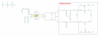
Other Parts Discussed in Thread: ADS5294, THS4551, ADS5294EVM
Tool/software:
Hello,
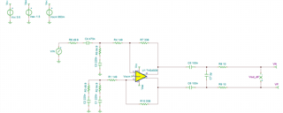
I want to convert a 0.9V single-ended signal to a 2Vpp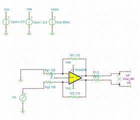
differential signal using the THS4509 and then connect it to an ADS5294 ADC.
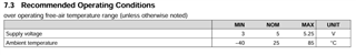
Is it possible to achieve a full-scale range in the ADC by configuring it as shown in the diagram Above?
If possible, could you please confirm how it should be configured to achieve this?