This thread has been locked.

If you have a related question, please click the "Ask a related question" button in the top right corner. The newly created question will be automatically linked to this question.

OPA2228: OPA2228

Part Number: OPA2228
Other Parts Discussed in Thread: OPA1612, OPA2350, OPA2227, OPA2140, OPA2192, OPA192

Tool/software:

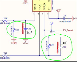
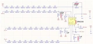
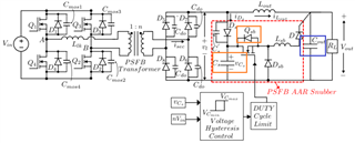
I am facing a problem with the differential amplifier circuit using OPA2228U (U6A). The schematic is shown below.

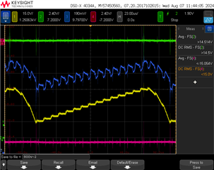
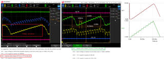
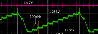
The input (Snub_Cap w.r.t GND) to U6A opamp differential circuit is as shown below in the green waveform (the voltage levels are marked in the plot), but the output of U6A opamp(TP14 w.r.t TP15 (GND2)), which is in yellow, is showing an oscillation of 100kHz.

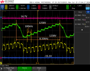
CH1 – Opamp (U6A) Output (TP14 w.r.t TP15) (YELLOW) 

CH2 – Input voltage to Opamp circuit (Snub_Cap w.r.t GND) (GREEN) 

CH3 – -15 V supply to opamp U6 (BLUE) 

CH4 – +15V supply to opamp U6 (YELLOW) 

The opamp U6B is also connected to a DC high-voltage signal, but its output is smooth and doesn't show any frequency content. 

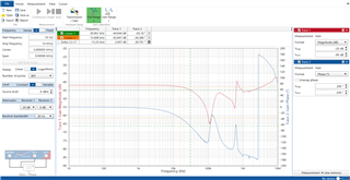
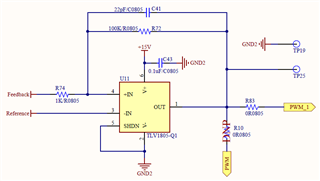
The feedback point (TP14) is then connected to a comparator, as shown below.

So, I am not sure why the output of U6A is showing such oscillations. Can somebody please help me out here?

Thank you

Vijaymahantesh V Surkod

  • Hi Vijay,

    The OPA2228 is a decompensated amplifier that is only stable for gains of 5 V/V or greater. As your noise gain is ~ 1V/V this configuration is inherently unstable and will oscillate as shown. You need to use the OPA2227 which is the unity-gain stable version of the device.

    As for your channel B not showing any frequency content, this is because you have populated 1μF capacitors which sets your bandwidth to ~8Hz. I would not expect to see much frequency content in this case. You will need to adjust these capacitors to set your desired cutoff frequency (Fc) according to the equation: Fc = 1/(2πRC)

    Regards,

    Zach

  • Thank you for the reply. Sorry for the delay. But I think OPA2227 has a very low slew rate. So, do you have any other recommendations for the opamps? How about the OPA1612 or OPA2350, or LMP8672MA? Something with a slew rate greater than or equal to 15V/us for the above application, having a noise gain of around 1.

    Thank you

    Vijaymahantesh V Surkod

  • Hi Vijay,

    I'm not sure that you need 15V/μs slew rate... The 330pF capacitor (C47) creates a low pass filter with the 2.49MΩ series input resistance resulting in a input signal bandwidth of less than 200Hz.

    Typically, the slew rate required can be calculated by the equation below. For 200Hz signal, your slew rate requirements should be fairly low.

    https://www.electronics-notes.com/articles/analogue_circuits/operational-amplifier-op-amp/slew-rate.php 

    If you do prefer an amplifier with a slew rate greater than 15V/μs, I recommend either OPA2140 or OPA2192. These are both 36V dual channel amplifiers in the SOIC package that can be used as a drop-in replacement on your board.

    See link to parametric comparison: https://www.ti.com/compare-products/?id=78&type=GPT&partList=OPA2140,OPA2192,OPA2228

    Regards,

    Zach

  • Hi Zach,

    As suggested, I had replaced OPA2228A with OPA2192ID (U6 in the schematics). But still, the problem persists

    CH1 – Input voltage to Differential amplifier Opamp circuit U6A (Snub_Cap w.r.t GND) (YELLOW) 

    CH2 – +15 V supply to opamp U6 (GREEN)  

    CH3 –  Opamp (U6A) Output (TP14 w.r.t TP15) (BLUE)  

    CH4 – -15V supply to opamp U6 (PINK) 

    and I replaced the C27 and C47 with the 220pF capacitance. With C27=C47=220pF and R1=R31=20k Ohms, the cut-off frequency for the differential amplifier filter will be 36.17 kHz (1/(2*pi*20k*220pF)).

    I have also got OPA2140AID. Do you suggest I replace U6 with OPA2140AID?

    Thank you.

    Vijaymahantesh V Surkod

  • Hi Vijaymahantesh,

    It looks like that input of the difference amplifier has close to 90kHz ripple frequency. You will need to have at least 1/10th to 1/20th LPF to get rid of it. 2nd order LPFs will be better than the single order. My guess is that you want to obtain a lower ripple filtered output signal to do some comparisons.  

    Also, please use 1uf low ESR bypass capacitors at +15Vdc and -15Vdc rail. low ESR means that ESR of 1uF < 10mOhm range. This will clean up the voltage spikes at supply rails. Put bypass caps next to the supply pins with a low noise ground. I think that you are sampling the current across shunt from a high voltage  switching supply. 

    OPA192 Difference Amplifier 08072024.TSC

    Please let me know if this helps. 

    Best,

    Raymond 

  • The differential amplifier is used to sense the voltage across the snubber capacitor. The Yellow waveform is the voltage across snubber capacitor. The yellow waveform is as expected, i.e it charges every 100kHz. But the differential amplifier output should have just attenuated and followed the input. I am adding the simulation file below. The feedback capacitors I have kept it to be 220pF. In my original question (at the top), I had posted a figure marking the necessary details. 1nF feedback capacitor will not work as the cut of frequency is way to less. 

    The simulation file below works perfectly fine (do run it with initial conditions), without any ripple at the output. 

    OPA2192ID_Differential_Amplifier.TSC

  • Hi Vijaymahantesh,

    But the differential amplifier output should have just attenuated and followed the input. I am adding the simulation file below

    Ok, it seems that the circuit is working now. OPA192 is a good op amp to use. 

    If you have additional questions, please let us know. 

    Best,

    Raymond

  • No, It is not working still. I have replaced the power supply capacitor to 1uF. But still in the hardware the same output voltage swing is present.

  • Hi Vijaymahantesh,

    I have replaced the power supply capacitor to 1uF

    Did you use low ESR capacitor? Please show me the plot power rails after low ESR 1uF is used (use MLCC 1uF capacitor for the best results). The plot's assigned channels are not consistent...

    Please restate your persisted problem. Using OPA192, I do not see the oscillation in the captured plot, and the output signal is shown as simulated. 

    You are monitor the snubber's voltage across the capacitor. Did you wait for the system to reach a steady state in your HV power rail. I see two frequencies in the plot, one is close to 100kHz, other one is between 5.4kHz to 8.3kHz. What are low frequency from? I do not believe that this is is not oscillatory frequency. 

    What type of load did U6 drive? 

    Best,

    Raymond

  • I have summarized the problem in a pdf attached here. I found is a little difficult to write everything here. So I made a document of what the actual problem is and attached here as a pdf. Please let me know your thoughts.sensing_problem.pdf

  • I also tried to get the frequency response of the U6A differential amplifier circuit using Bode100, and the figure for the same is below. The bode 100 source is connected to snub_cap and GND, and CH1 of Bode 100 is connected to snub_cap and GND, and CH2 of bode 100 is connected to TP14 and TP15. The bode 100 FRA is shown in figure 1 and the differential amplifier circuit is shown in figure 2.

    Figure 1

    Figure 2

  • Hi Vijaymahantesh,

    I reviewed your write-up and start to understand what you are trying to do. 

    First of all, when I saw 100kHz in your ±15Vdc supply rails, I suggested low ESR 1uF capacitor to decouple OPA192's dual rails. This is to lower the ripples and spikes in your ±15Vdc supply rails; and it is not the solution to resolve the "voltage dip" across the Cs capacitor. Frankly, you should not observe the 100kHz switching spikes at ±15Vdc supply rails, if the the switching output stage is well attenuated by the LC filter of the low voltage rails. It is possible that these spikes are coupled in from somewhere. 

    Based on the scope screen shots, I think OPA192 difference amplifier is doing what is designed to do. The "Cs" voltage dips at output of OPA192 (U6A) are measured at approx. 90mV in amplitude. If you back calculate the voltage drop across Cs capacitor, the delta voltage is approx. 11.2Vpk. You should get high voltage probe and monitor the delta voltage across the Cs capacitor's terminal, you should see the voltage dip at approx. 11Vpk magnitude.   

    I do not know how well 2.49Mohm and 20kohm resistors are matched in the difference amplifier. You have to use 1% or better resistor tolerance in order to get rid of most of common mode noise. I would use 0.1% resistor tolerances due to the large Mohm values. 

    Our PRAMPS application team is specialized in op amps. So we are only able to help you with op amp issues. However, I will offer some clues as I read your explanation. 

    1. Make sure the Cout is sized properly and it has to be low ESR type. 

    2. There should be a Q at the Vout stage, and make sure that the output stage is dequed properly, where Q <1 (0.707 range). 

    3. This AAR looks like "lossless" snubber, some kind of resonance clamp. When the Mosfet/Qsb is off, the energy stored in Lsb is likely dumped to Cout and RL.  AAR snubber is a protection circuit, generally it should not be used as a part of feedback circuit (you only provide the partial swithing power supply schematic...). 

    4. When Mosfet/Qsb is On, Cs capacitor is being charged and dump AAR snubber's current to Cout/RL. 

    I do not know why Cs capacitor has a voltage dip during the charging cycle. Perhaps Vout node has lower voltage than Cs clamp voltage from the current spikes during the Off/On transitions. The simulation is unable to tell you anything about the dynamic transient conditions. All we are doing is simulating an ideal condition. If you feed the actual Cs input waveform into the generator, then you may see why (I hope that you know how to do that in Tina simulator). 

    I would suggest to put this circuit in LTSpice simulator, and put a fix duty cycle, say 70% to understand how the circuit works in open loop. (LTSpice can handle the switching power supply simulation better than Tina ver. 9). From the open loop simulation, you will understand how Cs should charge and discharge vs. duty cycles. I am fairly sure that OPA192's output stage is following the input voltage across the Cs capacitor. 

    If you have other op amp questions, please let us know.  

    Best,

    Raymond