Other Parts Discussed in Thread: ADS8344, OPA4277, DS25CP152, OPA189
Tool/software:
Hello,
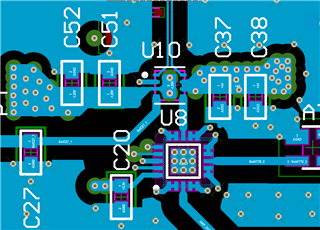
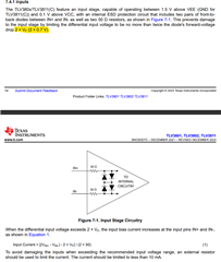
We have a fabricated circuit with TLV3801, DS25CP152, OPA189, OPA4277 and ADS8344 (see Figure 1.). TLV3801 (Figure 2.) is being used in a non-inverting comparator configuration with below power supply voltages -
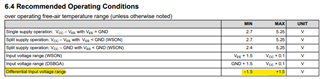
VCCI and VCCO = 4V
VEE = -1.25 V
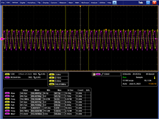
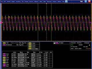
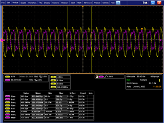
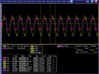
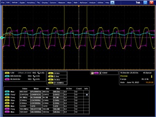
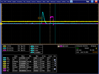
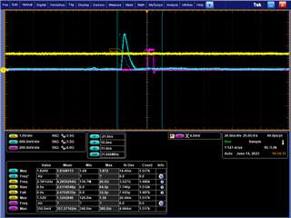
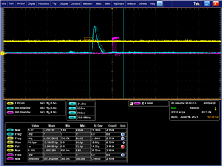
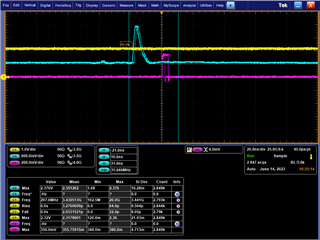
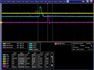
The non-inverting input is a 1 us 3.3 V pulse and the inverting input is DC voltage controlled via a resistor divider that consists of a resistor pot. The output of the comparator is logic pulse when probed at the Positive P arm of the LVDS pair output of DS25CP125 splitter and is inverted with respect to the input pulse. This is unexpected because of the non-inverting configuration of the comparator. The output of the comparator is as expected and non-inverted when short pulses of width < 1 us are connected to the non-inverting input. This is also probed at the positive P arm of the LVDS pair output of DS25CP125 splitter and the scope is 50 Ohm terminated with DC coupling.
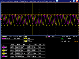
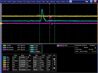
We replicated this configuration with TLV3801 evaluation board and could see correct output polarity w.r.t. input pulse polarity for 1 us 3.3 V pulse as well as shorter pulses < 1 us.
Could you please review the below custom circuit and recommend any changes and insights for this observed behavior, which is the output pulse polarity is inverted for wider pulses >= 1 us and correct polarity for shorter pulses < 1 us. Thank you
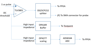
Figure 1: Overview
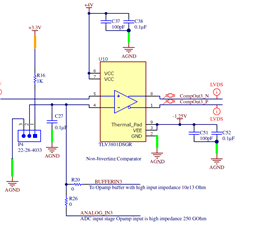
Figure 2: TLV3801
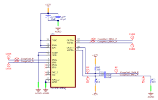
Figure 3: DS25CP152
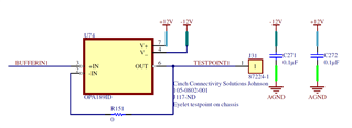
Figure 4: OPA189