This thread has been locked.
If you have a related question, please click the "Ask a related question" button in the top right corner. The newly created question will be automatically linked to this question.
Tool/software:
Hello
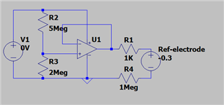
We are targeting to use the TLV8542 or the OPA2391 into our design to interface a high impedance accumulator (>100 mega ohm impedance accumulator)
when our device is in storage mode, the amplifier is not powered,
we use is as a non inverting amplifier with unity gain to buffer the signal into our system, the accumulator (+/-0,3VDC) is directly connected to the IN+ of the amplifier,
please can you share data about the capabilities of the TLV8542 and the OPA2391 to maintain the performances on the bias current when the device is not powered
looking forward for your support
best regards
The inputs of both the TLV8542 and OPA2391 have clamping diodes to V+. If the input voltage is more than 0.3 V or 0.5 V above V+, then a current flows through the diode, and if the current reaches 10 mA, can damage the device. (Also, this current into V+ can (partially) power up any device conntected to V+.) To avoid this, use a switch to disconnect the opamp input, or use an opamp with shutdown pin and keep it powered.
But if the input voltage is less than 0.3 V above V+, then no noticeable current will flow.
Ziad, I agree with Clemens. The "bias current" of a CMOS amplifier is the leakage of the input ESD structures. When the amplifier is not powered and you apply an input signal less than 0.3V you are putting a small forward bias on the diode. However, the knee of the diode curve where the diode is fully on will not happen until the input is greater than 0.3V. However, with Vin < 0.3V and the amplifier is not powered the bias current is no longer defined and may be larger than the specified bias current. However, I would not expect high currents in this case.
Best regards, Art
Thanks Clemens & Art
i have the same question for the output impedance when the TLV8542/OPA2391 is off ( not powered)
in our case one of the amplifier is buffering the high impedance electrode, and the output of second one is powering the high impedance reference electrode ( via non inverting unity gain amplifier - buffer),
when the system is in storage mode, there is no battery in the system, so the amplifier is off, in case our reference electrode has a potential between -0,3 and + 0,3V, is there any possibility of reverse leackage current thrue the amplifier output , our reference electode can be emulated as a battery with µAH capacity?
here is the deign
in other world can we have an idea about the current going thrue R1 when the device U1 is not powered? we need to avoid discharging our reference electrode
Thanks in advance for your support
best regards
Zaid,
When an amplifier is not powered the output impedance will not be zero. In most cases we do not charactered the output impedance of devices in the off-state. To get an amplifier with a high output impedance you may want to use an amplifier with a disable feature that is designed to have high output impedance when disabled. Note that not all amplifiers with a disable feature will have high output impedance. OPA334 is specifically designed with this feature in mind. Here is an E2E post discussing this topic: E2E on output leakage of OPA334 . In your case, you may find the your current design has acceptable leakage current as your signal level is quite low since this voltage level is low enough to avoid turning on any diode much.
Best regards, Art
Thanks for your feedback
can we have the inernal block diagram of the TLV8542 and the equivalent circuit ?
best regards
Zaid,
I cannot give you much detail as this is proprietary. I can say that it would have ESD protections structures as is shown below. Also, it is a rail-to-rail CMOS input / output so this document shows the basic input and output structure and explains how it works: Op Amp Input and Output Swing Limitations
Best regards,
Art