This thread has been locked.

If you have a related question, please click the "Ask a related question" button in the top right corner. The newly created question will be automatically linked to this question.

INA186-Q1: Abnormal Output

Part Number: INA186-Q1
Other Parts Discussed in Thread: INA186

Tool/software:

Hi Expert,

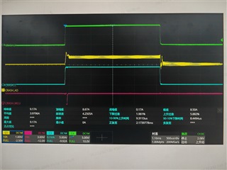
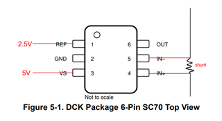
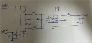
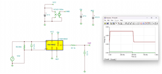
Customer is using INA186A2QDCKRQ1 in current sensor application. The waveform is described as below and pls ignore the green line and red line. When the current folws from IN+ to IN-, there was jitter in optput. While the current flows from IN- to IN+, the output works normally. Can you give some suggestions to troubleshoot it?

IN+ to IN-; OUT to VS;

  • Hi Expert,

    1. When the output extends the limit, whether the jitter will happen? 
    2. Can you simulate the schematic in Pspice and send me the file?
    3.  How to avoid the issue in application?

    My Email: beida-song@ti.com

  • Hi Beida,


    This looks like a common mode transient response. What is connected to the output of the INA? I suspect there's too large a capacitor which is causing this spike in the output. As per the datasheet, the largest value of capacitor on the INA output is 1nF, anything more will cause the ringing we see in the scope shot. I'm attaching a simulation file that shows the ringing when capacitor value is greater than 1nF and how it'll look at 1nF and how to overcome the ringing if you cant change the capacitor - by placing a large resistor at the output before the capacitor.


    INA186_jitter.zip

    Best,
    Mallika Senthil

  • Hi Mallika,

    Thanks for your strong support!

    1. When I simulate by customer's schematic, there is no fault appear. Customer's schematic as below:

    As your description, customer has already added 1k resistor in output side. Do you simulate for customrt's schematic?

    1. When the ouput extends 5V, the output appears spike. When the output < 5V, the output waveform is normal. Though the output extends the limit, the output should be stable voltage. Can you give some suggestion?
    2. Whether the cap isolation featuer is related to output jitter?
  • Hi Beida,

    Having 2 capacitors in series on the output might be the cause of this ripple in the output. Please share your simulations so I can take a look. Moreover, your supply is 5V, when output exceeds supply, device will malfunction.

    Best,
    Mallika Senthil

  • Hi Beida,

    Your simulation depicts the most ideal case, you won't see any jitter since the output has been made robust with the resistor and capacitor. I'd recommend the customer reanalyze their output after removing the second capacitor. Also, please note, the output range as specified in the abs max table.

    When the ouput extends 5V, the output appears spike. When the output < 5V, the output waveform is normal. Though the output extends the limit, the output should be stable voltage. Can you give some suggestion?

    Please ensure this output voltage is within range.

    Best,
    Mallika Senthil

  • Hi Malika,

    1. Can you give an explanation why the output capacitor is < 1nF?
    2. If you see the waveform, you can find the output is 3.5V when the input is 9A*20mΩ=180mV. In fact, the output is 0.18*50=9V, which extends the VS. Though we think the output should be 5V, the waveform displays the output is 3.5V, which is abnormal. Customer can't understand that.
    3. Customer remove the two output capacitors, there is no change for output voltage.
  • Hi Beida,

    Can you give an explanation why the output capacitor is < 1nF?

    The output impedance of most amplifiers limit the capacitance they can drive without oscillation. Please see the following app note for more information.
    https://www.ti.com/lit/an/sboa443/sboa443.pdf

    If you see the waveform, you can find the output is 3.5V when the input is 9A*20mΩ=180mV. In fact, the output is 0.18*50=9V, which extends the VS. Though we think the output should be 5V, the waveform displays the output is 3.5V, which is abnormal. Customer can't understand that.

    I'm looking into this, I'll get back to you soon.

    Best,
    Mallika Senthil

  • Hi Mallika,

    For the second question, do get the any idea?

  • Hi Mallika,

    Customer told me that the input signal gnd is not the same GND. So the input voltage of INA186 is float gnd. Can you simulate the condition?

    A strong phenomenon:When the input current (8A) is positive, the output is normal. When the input current(8A) is negative, the output is abnormal.

  • Hi Beida,

    Thank you for your patience, given the new information, I'll rework my simulation and get back to you.

    Best,
    Mallika Senthil