TLV3801: Non-linearity of voltage divider on non-inverting input

Part Number: TLV3801

Tool/software:

Hello.

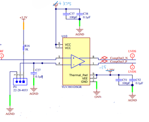
We have a TLV3801 with a non-inverting input range of 0 - 4.1V as a requirement. We are attempting to voltage divide the range to 0 - 1.5V so that the input differential stays below 1.5V. 

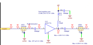
Fig1. Schematic of non-inverting input.

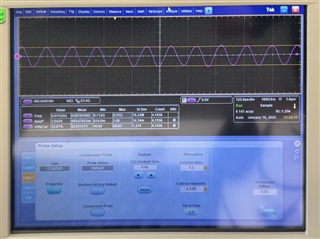
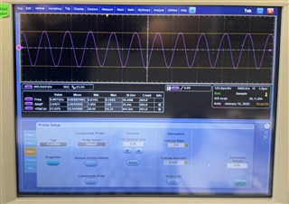
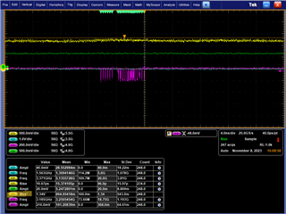
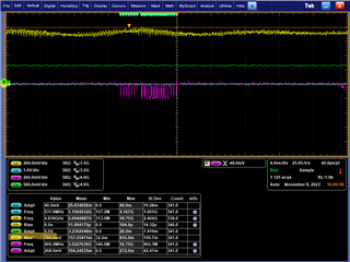
We replaced ATT8 in the figure with the voltage divider. We chose 49.9 Ohm and 86.6 Ohm resistors which should result in a ratio of ~.365. When testing the setup, we used a 800 Mhz sine wave with amplitude 1V. The output of the amplifier was 1.4V which was divided down to 640 mV. This is a ratio of ~.457. We tried a higher amplitude afterward and the circuit divided 2.4V to 1V, a ratio of ~.417. Could this non-linearity be caused by the comparator? Thanks for the help.

  • Hello Nirei,

    Can you show the comparator schematic? Particularly how you are DC biasing the input?

    Is there a DC path for the input? If you are AC coupled, how are you setting the "center" of the waveform?

    If the input is swinging around ground, then most likely you are being clamped by the ESD diodes on the negative swing.

    Is the waveform distorted in any direction?

  • Hello Paul,

    Here is the schematic for the comparator. We have a 1k resistor in series with the inverting input not pictured. The comparator outputs are also switched on the schematic but not on the physical board.

    Fig2. Comparator Schematic

    The inverting input is connected to a dial and the range is 0 - 2.7V. 

    We also tried a negative square wave input. The amplifier flips it, so the input voltage differential is <1.5. We still noticed nonlinearity and an incorrect voltage divider ratio.

    We did notice ringing distortion but only at low frequencies (~ 1 Mhz). This is out of spec for us as we require frequencies closer to ~1 Ghz. 

  • Hi Nirei,

    Just to clarify, the inverting terminal is connected to a low impedance source that ranges from 0 to 2.7V through a 1kΩ resistor.

    The input source is a 0 to 4.1V signal that gets voltage divided down with 49.9Ω and 86.6Ω resistors and connected to the non-inverting terminal.

    The power supply to the comparator is as shown: VCC = 4V and VEE = -1.25V.

    Could you confirm if there's a 100Ω termination resistor between OUTP and OUTN?

    In addition, could you please share some scope shots of the nonlinearity and incorrect divider ratio?

  • Hello,

    Sorry, I forgot to fix the schematic. We modified VCC to 3.75V and VEE to -1.5V. Everything else is correct. The outputs are connected to the below crosspoint switch which has internal 100 Ohm termination. 

    Fig3. Crosspoint Switch

    I will share scope shots soon. 

  • Hi Nirei,

    I see. I remember this circuit from your previous post.

    Please share the scope shots with us so Paul and I can analyze them. Please also include what each channel on the oscilloscope corresponds to which node on the schematic.

    Thanks,

    Ho

  • Hi Nirei,

    Please reopen this post if you have any updates.

  • Hello,

    Apologies for the delay in response. Unfortunately, we won't be able to share screenshots until next week.

    To provide some context, we've decided to scale the signal externally, outside of the board, to allow for greater flexibility in dividing input signals. As a result, the voltage divider is no longer an issue, but we have kept it for testing purposes. However, we did encounter another problem.

    We are currently testing with three different channels:

    1. One channel is configured exactly as shown in Fig.

    2. Another has the voltage divider replacing the attenuator (Fig. 4).

    Fig4. Voltage Divider CIrcuit

    3. The third channel has a 100 Ohm pull-down resistor instead of the attenuator. We added this because we observed a DC offset in the input. After the threshold voltage on the inverting input (the comparator’s reference) exceeds the non-inverting input, the comparator output would disappear once we probed the non-inverting input. We believe that probing the input introduced a grounding effect even with the high-impedance probe. We chose a 100 Ohm resistor because, together with a 10,000 pF capacitor, it creates a cutoff frequency of 159 kHz, which allows signals in the GHz range to pass through.

    Fig5. High-pass filter circuit 

    During testing, we encountered an issue: the threshold still needed to be around 1.4 times greater than the peak of the non-inverting input for the comparator to stop outputting. For example, with a 1V input on both the high-pass and 0 dB attenuator channels, the threshold needed to be about 1.4V for the output to disappear. We also tested with a 900 mV input, and the 1.4 scaling factor was still present.

    For the voltage division channel, the 1V input was divided down to 400 mV, and the threshold needed to be around 550 mV. In all cases, the output width gradually decreased as the threshold was increased. The general shape of the input and output waveforms is shown below.

    Fig6. General shape of comparator input and output waveform

    We know the high-pass filter channel resolved the DC offset issue, as probing this circuit while the threshold was above the input signal did not cause the output to disappear. 

    Our main question is: what could be causing this 1.45 scaling factor?

    Thanks for your help!

  • Hi Nirei,

    Let's confirm a few things before we look take a look at the scope shots next week. In Fig 6., are the threshold and input are both measured at the inputs (pin 4 and pin 5) of the comparator and referenced to VEE (pin 3 and pin 9)? In addition, could you please use a DMM to make sure that VCC referenced to GND and VEE referenced to GND are stable and the voltages are what we expect(4V and -1.25V)? In addition, please make sure that the oscilloscope you are measuring the signals with has the correct probing setup, that is, the signals are not visually gained up from the probing setup.

    The reason I am asking this is because in the example where the threshold is 1.1V and the input peaks to 1V, the output of the comparator shouldn't toggle as a 100mV differential is enough to overcome any internal hysteresis or offset that may lower the switching threshold. We should try to eliminate possible power or measurement issues first.

    One more thing, is the output as shown in Fig 6. a differential output, or are you just measuring one of the outputs (OUTP or OUTN) with respect to GND?

  • Hello,

    n Fig 6., are the threshold and input are both measured at the inputs (pin 4 and pin 5) of the comparator and referenced to VEE (pin 3 and pin 9)?

    The inputs are measured at pin 4 and pin 5 with respect to ground. 

    In addition, could you please use a DMM to make sure that VCC referenced to GND and VEE referenced to GND are stable and the voltages are what we expect(4V and -1.25V)?

    The voltages should be stable. However, they are are 3.75 and -1.5, I forgot to modify the schematic.

    In addition, please make sure that the oscilloscope you are measuring the signals with has the correct probing setup, that is, the signals are not visually gained up from the probing setup.

    We are using high impedance probes. The signals should not be affected. 

    One more thing, is the output as shown in Fig 6. a differential output, or are you just measuring one of the outputs (OUTP or OUTN) with respect to GND

    We are measuring OUTN with respect to GND.

  • Hi Nirei,

    Thanks for the quick response and details.

    I really appreciate your help in confirming the measurement setup.

    When I was talking about the probing setup, I was referring to the probe setup on the scope instead of the physical probe that you are using. I'm just making sure that the channel you are using is configured with the correct attenuation factor so that what we will see on the scope is what is physically present.

    To give an example, I'm using a 1x probe to measure a 1Vpp sine wave here:

    I set the attenuation to 0dB as there is no attenuation on a 1x probe, so the oscilloscope reflects a 1Vpp sine wave as expected.

    Without changing anything physically, I set the attenuation to 6db (2x):

    You can see that the oscilloscope now shows a 2Vpp sine wave, which is not what is physically being measured.

    I wanted you to check this to ensure that there is no 1.45 scaling factor on your probing set up on the oscilloscope channel(s) that you are using.

    Please also note that high impedance passive probes do have a loading effect on the input of the TLV3801. High impedance probes have an input capacitance associated with them, and this causes a low-pass effect which means that the probe has a finite bandwidth.

    800MHz is fairly high frequency, so please check that the probes have sufficient bandwidth.

  • Hello Ho Siu, 

    We should have the correct attenuation factor. Here is a picture of one of the channel settings on our scope.

    Fig7. Image of scope screen

    Our probe should also have sufficient bandwidth. Here is a picture of its specifications. 

    Fig8. Image of probe used

    Is it possible that the 1.4 scale factor could have something to do with the 1.4 voltage differential on the diodes? I feel as though the number being the same is probably a coincidence, but I want to hear your thoughts.  

    Thanks for the help. 

  • Hi Nirei,

    The oscilloscope setup looks fine to me.

    I did notice the 1.4V being the double diode drop that limits the voltage across the inverting and non-inverting terminals as well. However, from what you've described here:

    the 1V input was divided down to 400 mV, and the threshold needed to be around 550 mV

    It seems like the "offset" for the threshold is still present even if the differential (IN+ - IN-) is nowhere near the 2x forward voltage limit.

    Just to confirm, on the images with the comparator, the inverting terminal is driven by "pot." Is this a low-side pot that sets a voltage divider to set the threshold? If so, what's the resistance of the upper resistor?

    I don't want to speculate too much without seeing the signals themselves. It'd be great if you could share the scope shots next week after the holiday so that Paul and I could take a look.

  • Hello Ho Siu,

    The pot does set a voltage divider. The upper resistor is shown in Fig2 (R16) and is 1k. 

    We should have scope shots for you soon. 

    We had another thought regarding the channel:

    The channels are specified for 50 Ohm impedance matching. ATT7 and U12 (the amplifier) are both 50 Ohm matched. The TLV3801, however, would have a high input impedance much greater than 50, correct? Could this mismatch explain some of the issues we were facing?

    Thanks for the help.