- Ask a related questionWhat is a related question?A related question is a question created from another question. When the related question is created, it will be automatically linked to the original question.
Tool/software:
Title: Op-Amp Behavior Differences After Repeated Use: Could It Be Soldering or PCB Material Issues?
Hello Team,
I am facing an issue with two identical buffer circuit boards, and I’m trying to understand why their performance differs. I suspect it might be related to either the handling/soldering process or PCB material. Here are the details:
Setup:


Observations:
Questions:
Below are the test results from both boards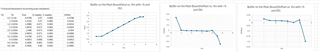 2nd board result:
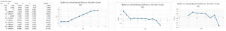
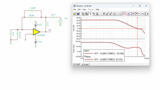
First board result

Could this behavior be due to handling or soldering issues?if soldering might be the issue can you please tell me what precautions to take care(Temperature etc). For example, is the op-amp being damaged during assembly or subsequent handling? while handling i am making sure of ESD protection.
so can you please help me where it is going wrong in simple buffer mode?


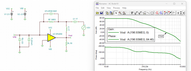
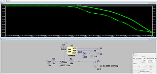
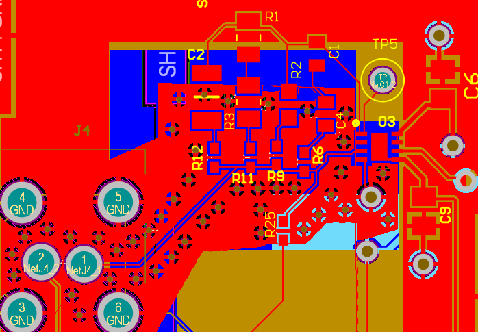
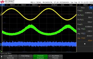 so yellow color graph is input which i gave from function generator , green color graph is the output of teh opamp where the sc is 1.36 .. and please ignore blue color graph , and the circuit layout diagram is attached