OPA847: Large overshoot and oscillation problem on my TIA amp.

Part Number: OPA847
Other Parts Discussed in Thread: DEM-OPA-SO-1A, TINA-TI, , LMH6629, LMH32401

Tool/software:

Hello,

I’m a beginner with transimpedance amplifier design.

APD:

- Photocurrent: pulses of a few µA, width on the order of 10 ns

- Intrinsic capacitance: ~22 pF

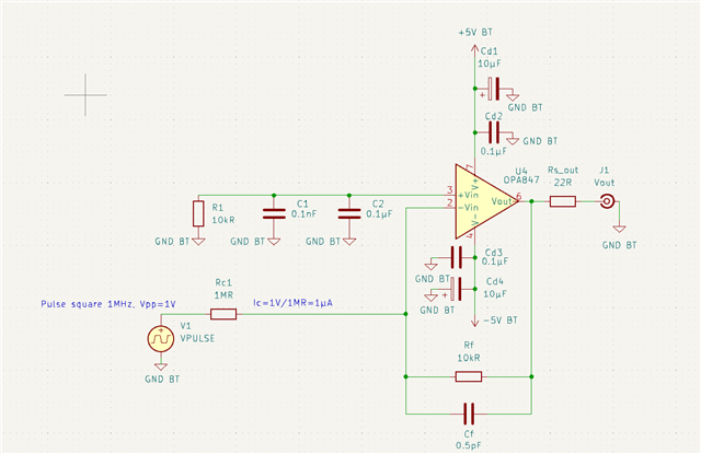
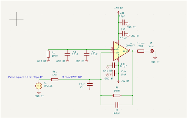
For now, I’m only at the simulation stage, working on developing a stable TIA circuit without actually using my APD. So instead, I’m using a function generator to produce 1 MHz square pulses, and right after the input I place a 1 MΩ resistor, which gives me a current of 1 µA.

I estimated the total parasitic capacitances at the input to be about 28 pF.

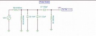
I used the TIA_calc Excel calculator to check my calculations.
I need a bandwidth of 40 MHz, so a feedback resistor of 10 kΩ and a feedback capacitor of 0.5 pF seem appropriate (I subtracted 0.2 pF from my actual Cf value to account for the internal capacitance of the resistor, which is 0.2 pF).

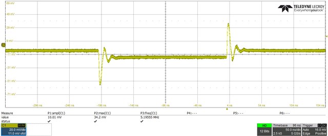
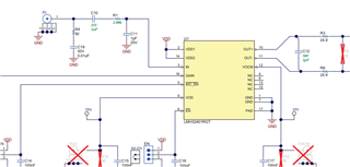
I built this on a DEM-OPA-SO-1A board suited for TIAs, and I do get a square signal.

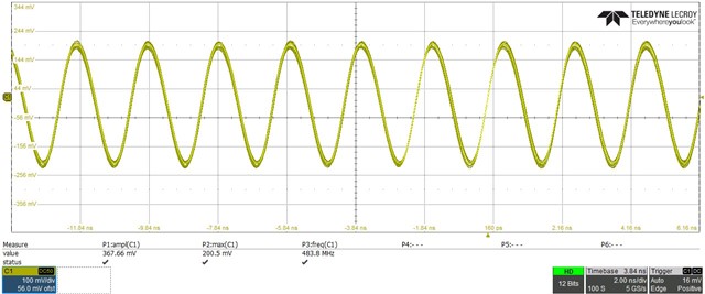
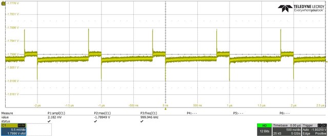
The big issue is that I have a very large overshoot regardless of the setup (on the order of several hundred percent) and when I try to set a feedback Cf (0.2,0.3,0.5pF) it goes straight to oscillation.

Also, if I try to adjust the Cf values, my system starts oscillating badly, and I don’t really understand why...

I’m attaching my KiCad schematic and the Tina-TI file (I’m not very familiar with this software, I did my best), along with oscilloscope screenshots of my output.

Thanks.

   opa847_10kR.TSC

  • Hello Joe,

      Thank you for using our calc tools and for all this helpful information!

      You are correct in the debugging method for TIAs. The reason it is oscillating is because I believe you forgot to include the PD input capacitance you used to calculate your design, the 22pF cap should be right at the input of the amplifier VIN-. This input capacitance to ground is used to apply the pole/zero creation + interaction with the feedback resistor/feedback capacitance in order to achieve a stable system since the PD is not being used for initial testing. It will shape your noise gain in the higher frequencies to achieve at least a gain of 12 V/V for amplifier stability. Once PD is used at the input for your final design, this capacitance will be at the input of the VIN- and work in a similar way in the system, 

      Also, you are at the right thought process on testing without a PD, but the best way we found in testing with a function generate is via this method: 

       This will help achieve proper 50ohm impedance matching at the source to minimize power reflections. 

    • At higher frequencies, the capacitors short out and the network analyzer see its desired 50ohm termination.
    • The caps act like a current divider sending a small portion of the current through the series 50ohm into the series cap that connects to the circuit under test.
    • The apparent source impedance looking back into the circuit becomes the series capacitor at high frequency

      Here is an e2e thread on this same topic with more details. The links in the response do not work, but the summary I gave after the response is the same information: e2e.ti.com/.../opa818-testing-tia-without-photodiode.

      Also, as a simpler quick method, you can use the same values as below from LMH32401EVM, which shows how to test with a voltage source if no current source is available. The LMH32401 as integrated feedback capacitance to keep amplifier stable, this will need to be added for LMH6629.

       Overall, you should try adding the input capacitor of 22pF to ground at the IN- node of the amplifier. Then, you can look into the second part for optimizing testing with a function generator. 

    Thank you,

    Sima

  • Hello Sima, and thank you a lot for your reply,

    I’m not sure I fully understood everything, so please excuse me for asking somewhat basic questions.

    I tried adding a 22 pF capacitor between In– and GND as you suggested, but during testing on my bench I ended up with a signal that oscillates (see attached updated schematic and signal) and the overshoot grow a lot.
    Perhaps I misunderstood your message and the capacitor should only be added when testing with the photodiode? What I did was based on what is shown in the TI OPA847 documentation for a transimpedance configuration. Should I understand that these example circuits are not necessarily complete?

    Regarding the simulation setup you described, thank you very much — I haven’t yet had the time to implement it but I will give it a try.

    One 2 more questions: what is the purpose of the series resistor Rs_in that is sometimes added on the PCB before the In– input? And how to choose the capa on the In+ (C1 and C2 in my case), i have not found anything. It was the documentation values.

    Thanks!


  • Hello Joe,

      No worries they have been good questions + clarifications!

    1.  Yes, you understood me correctly, the advice was to add the 22pF from IN- to GND if you do not have a photodiode at the input. When you have the photodiode at the input, then you would remove this capacitor since this value will now come from the photodiode. If it is still oscillating, how close is the 22pF capacitance to IN-? Maybe, we can try stabilizing this circuit further than calculated, would you be able to try changing out feedback capacitance to 1pF. This will reduce the closed-loop bandwidth, but could help in the debugging process for the moment. 

    2. Rs_in (RISO) that is usually suggested in the layout sections of our amplifiers is a small resistor to dampen the potential resonance caused by the trace inductance and the amplifiers internal capacitance and reduces the inductive isolation between the APD and the feedback network. I have found that when others have followed this advice, it has not been very helpful and could cause more issues. I recommend not adding this resistor, and to instead place the diode/APD as close to the IN- pin of the amplifier as possible in your final design.
    3. To choose C1 and C2 from the original advice to test without a PD, C1 in combination with your 50 ohm matching impedance will act as a low-pass filter or a pole in the frequency response which compensates for the zero caused by the feedback capacitor/resistor. (Choose this based on your expected closed-loop bandwidth). And C2 will be your PD capacitance which is around 22pF.

      Below is a more advanced example to account for parasitic on board + any other issues in frequency response:

      1. The input side that was previously proposed works in order to simulate a photodiode input stage using a voltage source. The important aspect of simulating a stage like this would be to include the photodiode capacitance (C7 of 150pF). C8 and C1 with the resistor divider (R8 and R2) act as a low pass filter or a pole in the frequency response which compensates for the zero caused by C4 and feedback resistor (high pass filter).

        In this E2E thread (1,3), Michael and Kai went of the assumption that your source voltage (usually from network analyzer or signal generator) will have a 50 ohm source. So to impedance match this 50 ohm source (R8), you would need R2 at also 50 ohms. Then they chose C8 or C1 depending on your bandwidth requirements. C8 and C1 can be combined as parallel capacitors, they had this separated because it is good practice when making a test board to give yourself more pads incase tuning is needed due to parasitic. As a close estimate, you can use RC filter concept to determine capacitance for the input bandwidth, in this case they picked around in the low kHz.

        Increasing R8 and R2 came about because in the first thread, the higher input capacitance for C8 with 50 ohm matching led to issues with the passband increasing at higher frequencies due to the lack of feedback resistor to create that compensation. So, that is the reason 10nF was kept, but the resistors were increased using again RC filter concept to obtain the lower input bandwidth in the Hz.

        I use this calculate for an estimate: sim.okawa-denshi.jp/.../CRlowkeisan.htm. Then I use Tina-TI to simulate AC response to tune values. But Michael’s article that he linked “Here’s an Easy Way To Test Wideband Transimpedance Amplfiers” goes into detail on the transfer functions and calculating the capacitors to obtain maximally flat passband.

    Thank you,

    Sima

  • Hello Sima, and thank you very much for all the time you’ve dedicated, it’s very kind of you.

    I just got back to working on this.
    I was able to test what you suggested, but I have a few small points I’m not clear about. In your first point, you indicate adding a 22 pF capacitor to simulate my photodiode between IN- and GND. But in the more advanced example, I see that the 150 pF capacitor (22 pF in my case) is placed between the resistor Rs_in and the inverting input IN-.

    I must admit I’m a bit confused.
    I tried both cases:

    • Placing a 22 pF capacitor between IN- and GND results in strong oscillations in the MHz range.

    • Placing the 22 pF capacitor between Rs_in and the inverting input IN- doesn't change much, but perhaps this does not correctly simulate a photodiode, because in the equivalent circuit of a photodiode, C_pd is between the photodiode input and GND.

    As soon as I add a capacitor (even 1pF) to either the IN+ or IN- branch and GND, the whole system starts oscillating. What's that supposed to mean?

    Here's my schematic, with the capa and resistors in red that I've tried to add one by one, but which make my whole system oscillate...

    Thanks 

    Joe