THS3217: Assistance with Differential Amplifier Design Issues

Part Number: THS3217
Other Parts Discussed in Thread: BUF802, OPA140, OPA2140,

Hi,

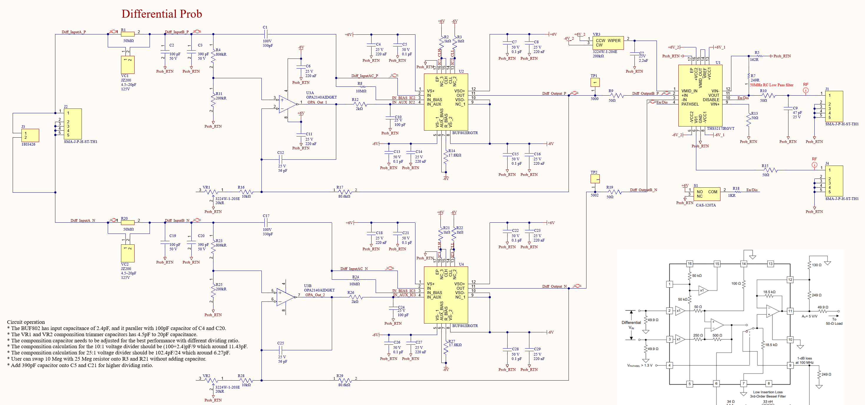
I have designed a differential amplifier using two BUF802s and a THS3217, and we have assembled a few boards for testing. The design includes two output options from the THS3217: VO1, which has no filter, and VOUT, which includes a 50 MHz filter. The performance has been excellent; however, I have encountered some issues that I would like to address for the next iteration.

When the board is not connected to the function generator (open input), it exhibits noise levels of approximately +/- 1.5 to 2V. Shorting both inputs together does not seem to have any effect. When the board is connected to the function generator, oscillations occur when the orientation of the cables is changed. We have replaced several cables, but this has not resolved the issue.

I am considering replacing (VR1 + R16) and (VR2 + R28) with fixed 20k resistors with a tolerance of 1% or 0.1%. Would this change have any negative impact?

Additionally, regarding R9 and R19, should I use 10 ohm, 50 ohm, or remove them entirely? The distance on the PCB is approximately 220 mils.

Thank you for your assistance!

Best regards,
WeyAnn Chen

image.png

  • Hi, 

    I need to update the measurement value from above. The noise levels of approximately +/- 200mV not +/-1.5V, and I did use differential probe measure across R9 and R19 which shows noise from output of BUF802. any suggestion? 

  • Hi WeyAnn,

    Can you share an image of what you are seeing? Is there a way to disconnect the resistors R9 and R10 to isolate the two stages and measure the outputs of the individual BUF802 outputs?  Replacing the pot with a fixed 20k would technically be ok. The reason for this potentiometer it to tune your response and allow for your low and high frequency cross over to be smooth and would ultimately keep your passband as flat as possible. It would be worth trying in your setup and see if this response is ok with your system. The reason for the 50-ohm resistors (R9 and R19) is primarily for impedance matching onto the next stage. However, considering how close the input stage of the THS3217 is, I would not think you need 50ohm resistors. You could reduce them to 10ohms just to have some isolation for any parasitic capacitance seen by the BUF802. I would suggest for future iterations, if you will have a test point, I would place this behind the 50ohms as probing these nodes could cause stability issues since the probe itself has capacitance. Placing these test points behind any series resistance would offer some isolation from the output of the BUF802.

    Best Regards,

    Ignacio

  • Hi Ignacio,

    Thank you for the reply, I will try your suggestion above. I did more testing last week, the output at TP1 and TP2 looks clean, but it shows10mV noise after R17 and R19. I think about instrumentation amplifier front end setup(see the picture below), and I wonder that at VR1 and VR2, should we connect return to each other instead to ground for differential input? can the CMRR error cause that noise issue? 

    Best Regards,

     Weyann 

  • Hi WeyAnn,

    Could you share where you probed and see this noise you mention. You mentioned directly at the outputs of the buffers you see no issue but after R17 you do. Where is after R17, is it at the node between R16 and R17? The noise does seem slightly high; does the signal you see look like an oscillation or does it appear like random noise?

    Best Regards,

    Ignacio

  • Hi Ignacio,

    The picture "Input_no_Connect1" is connect COAX cable to AWG without output signal, and the picture "Input_no_Connect2" is open no COAX.

      Input_no_Connect1

     Input_no_Connect2

    The two picture below shows that unstable output wit 20u pulse signal.

    I removed R9 and R19 isolated it from THS3217, and I input 20u pulse signal and measure the signal with end probe. 
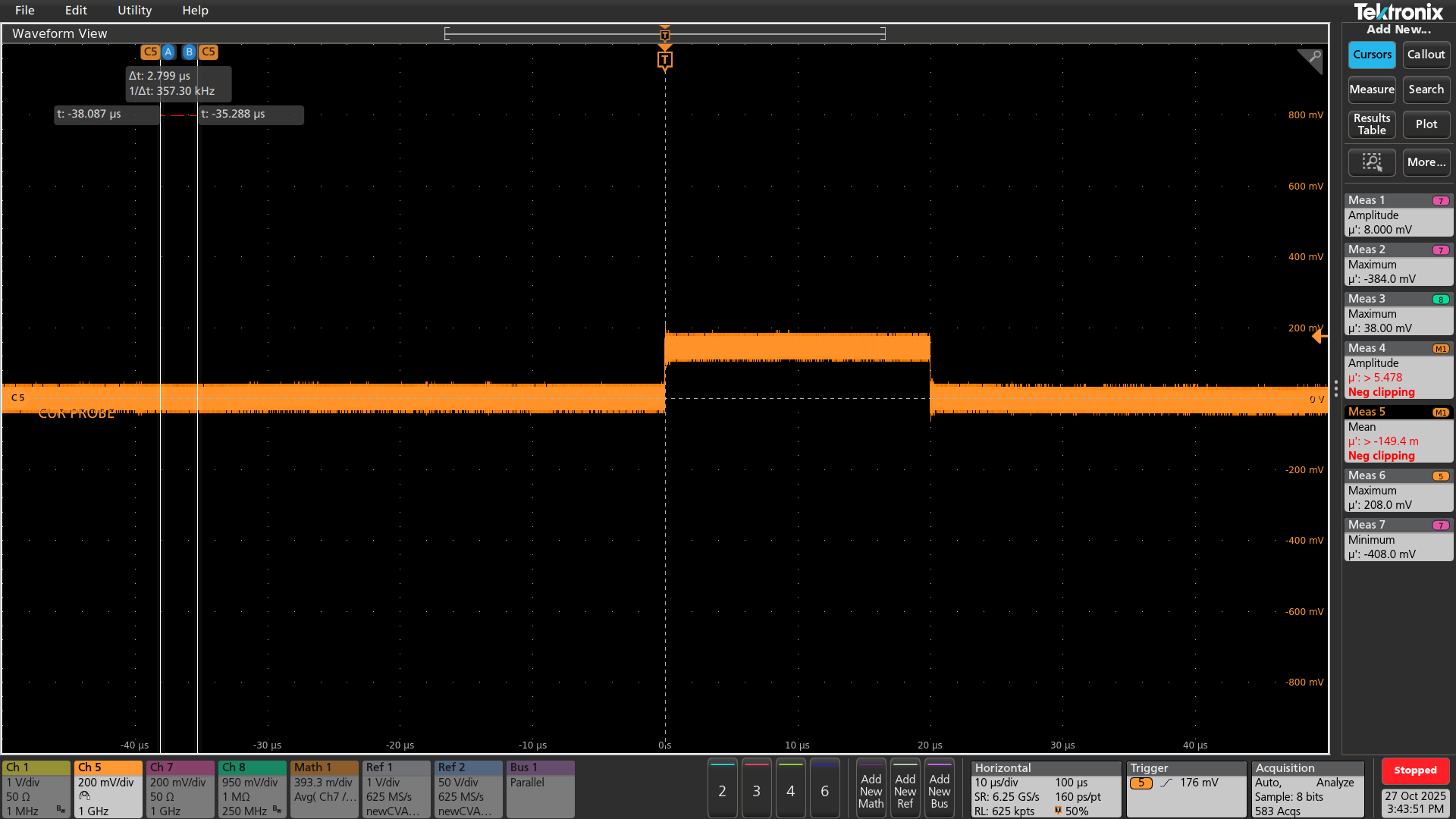
This is output at C2 

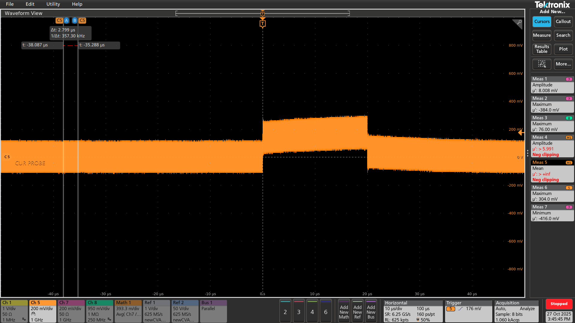
     This is output at TP1

    There is an interesting thing I found during this test, after my single end probe touched R17 pin1 then repeat the same measurement above, the signal become clean like below until I touch the TP1. 


    I wonder what can cause the feedback loop for OPA140 noise? and I use OPA2140 with .22uF decoupling capacitor, should I increase capacitance? Do you allow to have MS teams meeting? I will like speak with you if that is possible.

    Best Regards

    Weyann 

  • Hi Weyann,

    The input being measured at C2 seems very noisy. It is hard to completely rule out if its noise or an oscillation. We would need to zoom into the signal to see if there is some kind of repetition. Regarding the probing at the OPA140. It is hard to definitively say what is happening without confirming if it is oscillating. I do not think decoupling would make a difference. Have you tried sending this signal through our BUF802EVM and see if you experience the same issues?

    Best Regards,

    Ignacio

  • Hi Ignacio,

    The measurement at C2 is very noisy, but noise drop down after scope probe touch HF path at R10, and it stay less noise until I touch output of BUF802. The picture below shows before and after. I have two questions at this moment.

    1. The BUF802 CLH and CLL option since I have not use it, would that cause output error?

    2. I did look https://www.diva-portal.org/smash/get/diva2:1913874/FULLTEXT01.pdf which use same design base, they use 2x 10:1 divider before the BUF802. Would that setup perform better compare my setup?

    3. They use 30ohm resistor before C1, what is the purpuse of that resistor 

     Before

     After

    Best Regards

    Weyann 

  • Hi Weyann,

    The CLH and CLL are clamps and should not be causing any of these issues. When touching these different nodes, you could be changing the response due to parasitic capacitance on the probe. When probing the output of the BUF802 are you measuring on the right pad of R9/R17? I was unable to open the pdf you sent but I would recommend trying our BUF802EVM to confirm it is not something like layout causing these issues. We have a tested EVM that behaves as expected. I would highly recommend trying this to confirm you see the signal you would expect. The 30ohm resistor being used is to improve the S11 performance of the circuit and ensure the impedance looking into the input of the device is 50ohms at high frequencies. There is more information on page 23 of the BUF802 datasheet.

    Best Regards,

    Ignacio

  • Hi Ignacio,

    Thank you for the reply

    I installed that 30ohm resistor onto board before the C1, it does help clean out that noise and make it stable. I have some relate questions.

    1. For 50:1 attenuator, what is different by using single 50Mohm resistor compare with picture below? which you would recommend.

    2. For the board layout, should I remove ground plane/or all plane below the signal line? since it is differential prob.

    3. Should I use RF resistor for r10, R15, R9, R19...etc? what is benefit or disadvantage to use it?     

    4. Anything I should do/can improve overall circuit?

    Best Regards

    Weyann 

  • Hello Weyann,

      Ignacio is out of office and will be back on Monday. 

    Thank you,
    Sima

  • Hi Weyann,

    For your first question. The benefit I see with attenuating the way the image shows is to help tune the circuit better than if you just had one big resistor with a capacitor in parallel. It will allow you to have more knobs to tune the circuit as needed. I cannot think of other major reasons why one design is better than the other, not including the more obvious reasons like board space and extra components. For your board layout I would not recommend removing any ground plane under your signal traces. The ground plane under signal layers is critical to maintain proper signal integrity. Regarding the choice of Rf resistors, they would provide an overall benefit as these resistors behave better across frequency. I am not sure how much benefit they will provide in this design as we did not use Rf resistors in our design, but this should only help. The disadvantage would be the price and availability for different values. For improvements to the circuit, I would consider placing the test points behind some isolation resistors like we have discussed. Overall, the design is very similar to our design, but I can ask the team and get back to you.

    Best Regards,

    Ignacio

  • Hi Ignacio,

    Thank you for the detailed example, and I apologize for my late reply. I have been busy re-layouting the board and have moved most components to the top layer. If I send you the Altium file, would you be able to review my work? There are a few concerns I would like your input on:

    1. Component Placement: I am wondering about the locations of the OPA140 and variable resistors VR1 and VR2. Could my layout potentially have a negative impact?

    2. Variable Resistor Value: For the offset voltage adjustment on the THS3217, is a value of 200K ohms for VR3 variable resistor? Do you have any recommendations?

    3. Ground Copper Removal: The THS3217 datasheet recommends removing the copper ground under the differential input. Should I follow this guideline?

    Your expertise, along with that of your team, is invaluable to me, and I want to ensure that my design performs as well as your evaluation board or identify any areas for improvement.

    Thank you for your assistance!

    Best regards,

  • Hi Weyann,

    I spoke to a team member which supports the BUF802 device, and he will be able to look over the layout and give additional feedback. Looking at your THS3217, everything looks laid out as ideal as could be with your decoupling capacitors close to your device pins and multiple vias to ground. I would add more vias around your SMA pins that are grounded, I am not sure if I they are there, but I did not seem them. As far as the choice of wiper to tune any potential offset, this would be a good option as higher potentiometer values should offer finer tuning capability. You could reduce this to a smaller value, but I do not see why 200k would not be fine as long as you are meeting the power rating of the potentiometer. Regarding your question about the plane removal under the traces, I am not sure why the datasheet would say to remove these as this would be ideal to create a microstrip line and would likely do more harm by removing them. I would stick with leaving ground planes under and around the traces as this is ideal for high-speed signals. I am adding both the BUF802EVM and THS3217EVM users guides for reference below. These highlight both the schematic and layers, which would be the best reference for how we layout our devices to get the performance we get. Most of our suggestions and layout guidelines are captured in our EVMs which would therefore be your best reference.

    THS3215EVM and THS3217EVM (Rev. A)

    BUF802RGTEVM User's Guide (Rev. A)

    Best Regards,

    Ignacio

  • Hi Ignacio,

    Thank you for the reply. I will do the adjustment and send my Altium design file to thru email for closer look over.

     Best Regards,

    Weyann 

  • Hi Weyann,

    That should be fine. I believe my teammate will send his response through the thread but if there is any information that we can't capture from your images we can look at your files, but I believe most of the important parts of your design can be seen in the image.

    Best Regards,

    Ignacio

  • Hi Ignacio,

    I take your word add grounding plan and vias around output SMA. Do I need to add shielding via on output trace? I wonder that impendence can be mis-match without doing that. Do I need to do something(shielding via) on input SMA?

    Best Regards,

    Weyann 

  • Hi Weyann,

    We typically add a ground polygon on the top layer and add vias throughout the board. This is what we did for our BUF802EVM. I don't see a negative to doing this if space allows. This would be isolating signal traces and help with EMI. 

    Best Regards,

    Ignacio

  • Hi Ignacio,

    Thank you for the reply. I did little adjustment on the layout by swap the location of OPA140 (U1, U3) with capacitors (VC2, VC4) in order to limited feedback trace length. Thank you for all the great advice and help, hopefully would hear additional feedback from BUF802 team soon.

    Best Regards,

    Weyann 

  • Hi Weyann,

    I am looking into this, Please give me couple of day, will get back by Friday morning.

    Regards

    Anant 

  • Hi Anant,

    Thank you for the check up, I just post last updated above, please let me know if you need Altium file for review.

    Regards,

    Weyann

  • Hi Weyann,

    Can you share the altium file also?

    Regards

    Anant

  • Hi Anant,

    Do you have email that I can send over Altium file? I don't want everything post on forum.

    Weyann 

  • Weyann,

    I have dropped you an email, you can share the file share there.

    Regards

    Anant