A related question is a question created from another question. When the related question is created, it will be automatically linked to the original question.
If you have a related question, please click the "Ask a related question" button in the top right corner. The newly created question will be automatically linked to this question.
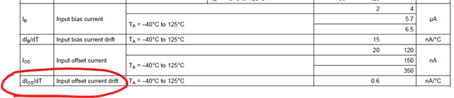
In some other datasheet, it is mentioned. eg, OPA2626
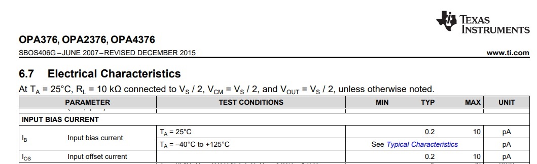
Does that mean the input offset current Vs temperature could be neglected in OPA2376.
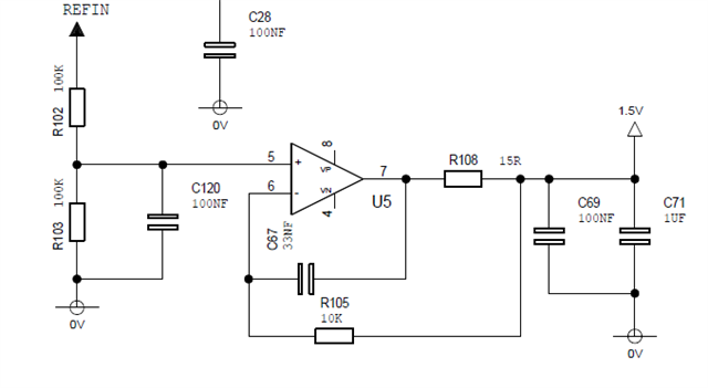
Actually, I found some temperature drift of the following circuit. It is roughly 36uV/C. I think I will change the resistor to 10kohm and check the result.
Maybe it is not from input offset current drift. Maybe it is from input bias current drift. I am not quite sure about this. And it is not on every sample. For most of them, the temperature drift is fine. But I do see some sample have this kind of behavior. I am trying to locate the problem.
The input bias offset current, Ios, and IB double every 10 deg C, thus 0.2pA at 25C will increase to 0.2pA*2^[(125C-25C)/10] = 0.2pA*2*10 = 200pA at 125 deg C. This is shown on the IB vs temp graph below.
However, what you may be seeing are the effects of the input current noise density, which is specified at 25C as typical 2fA/rt-Hz but may be as high as max 40fA/rt-Hz - see below. Since the input current noise is a function of temperature, as the temperature increase its magnitude will also increase.
From the analysis, I don't the the bias voltage drift is from the offset voltage drift or input bias current drift of OPA2376. I guess there is something behind this. I will try to figure it out. Actually, the problem I face is the bias voltage drift of the circuit. It is roughly 36.6uV/℃。
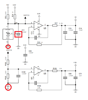
I have a reference voltage & bias voltage from OPA2376, the original reference voltage is LM4040.
I add another circuit to measure the current
If I do not inject any current, the problem is the measured value drift with temperature, roughly 0.2bit/℃. And I use a 14 bit ADC. So it is 36.7uV/℃。
I want to find out why the offset voltage drift with temperature.
The situation is a little bit complex. I will try to explain it in short. The problem is the offset voltage drift in the measurement circuit.
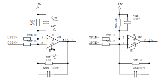
I use a 0.5mohm shunt to measure the current. I build a 2 stage gain amplifier you could see above. *10 gain and *133gain. These two are OPA2333 with DFN package. I choose this part as it is zero drift and the signal is DC. Zero drift is necessary especially for temperature drift.
The reference voltage and bias voltage also shows above. The amplifier is OPA2376 also due to low offset. The offset drift of OPA2376 is not low. But I believe it is not a problem due to it is only *1 gain.
I measure the output at the ADC side under different temperatures when no current is injected. I want to measure the offset voltage by the circuit.
The measurement of the offset voltage is directly by the ADC embedded in the Micro, a 14 bit SAR ADC with 3V reference voltage. I read the ADC value directly(average of 4000 samples, 2kSPS, total 2 seconds)
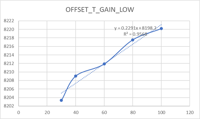
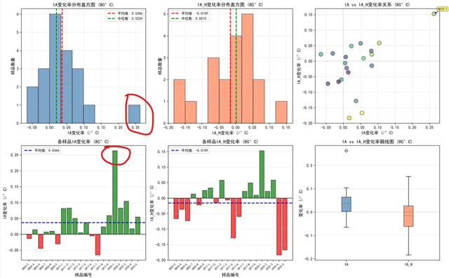
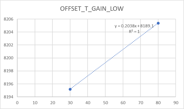
I measurement 23 samples, 2 of them have typical offset drift. It is 0.229bit per ℃
This is one of the result
Another bad sample is
So I require a full analysis of temperature drift of the whole circuit, include the reference voltage, bias voltage and measurement circuit.
I also will do some test on the bad sample for reason.
When we talk about the offset voltage drift, maybe we are talking about VCM = V+-1V(3.3-1=2.3V)
Electrical Characteristics table header has this text "At TA = 25°C, RL = 10 kΩ connected to VS / 2, VCM = VS / 2, and VOUT = VS / 2, unless otherwise noted" So the common mode is 1/2 of supply voltage. In our case 1.65V; it is in the flat part of the curve. The 1.5V channel is close to the trimmed production point
Within 1V of supply voltage (over 2.3V in our case), a different set of input transistors run the op amp. These different transistors are not as matched and offset is not trimmed out in production.
Within 1.3V of the positive rail, DC and AC specifications of OPA2376 and TLV2376 are much worse. This is especially true in case of temp drift, which increases to 25uV/C - see below.
Thus, close to positive rail I would recommend using OPA2392.
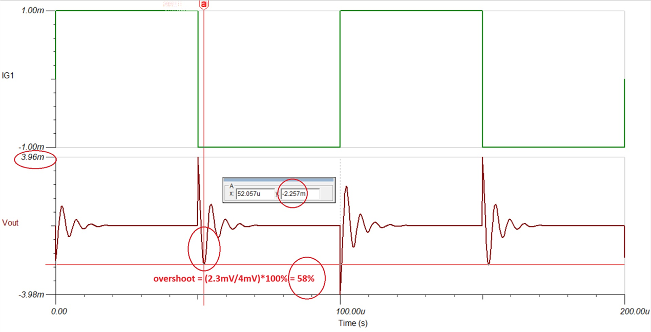
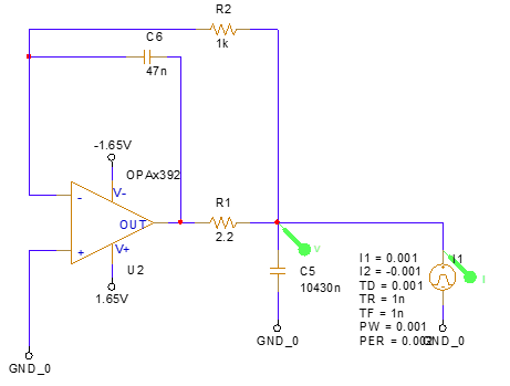
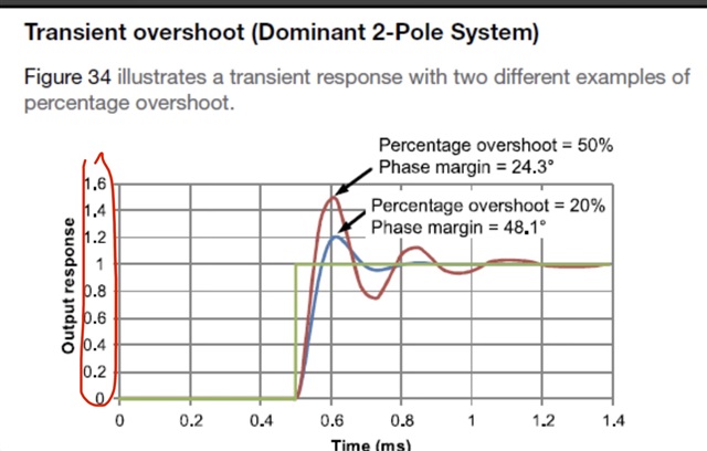
Transient simulation shows the circuit has 58% small-signal overshoot, which is way ABOVE maximum recommended of 25% - see below.
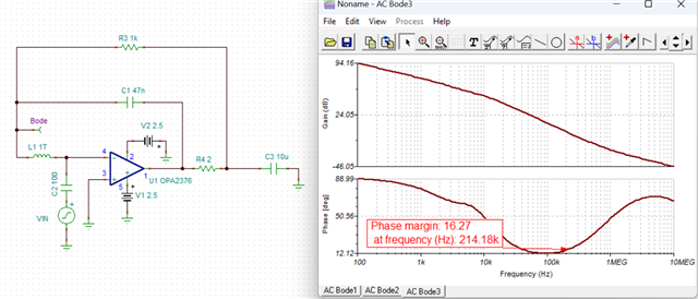
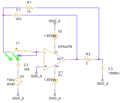
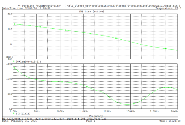
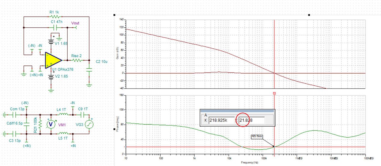
AC stability analysis show the circuit to be ONLY marginally stable with 22 degrees phase margin that is way below the minimum recommended 45 degrees.
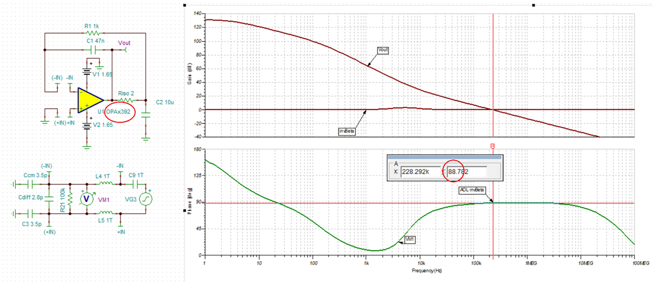
What ii all means is that over wafer fab process variation the phase margin may go down by 20 degrees and the circuit may be outright unstable or its setting time may be extremely long. This is yet another reason why you should instead use OPA2392 - see below.
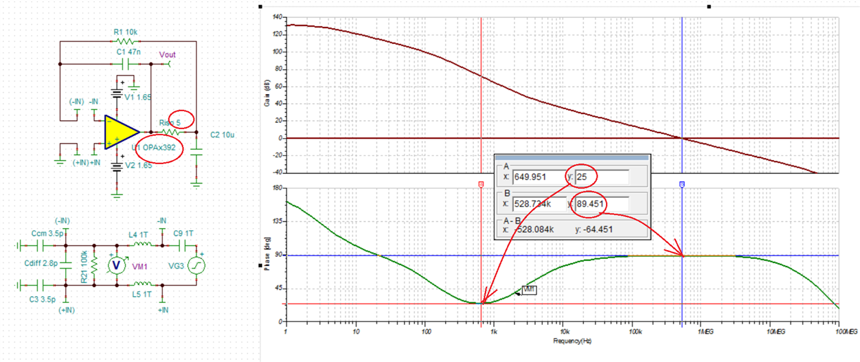
Having said that I would also increase Riso to 5ohm to lift the dip in the phase margin above 25 degrees - see below.
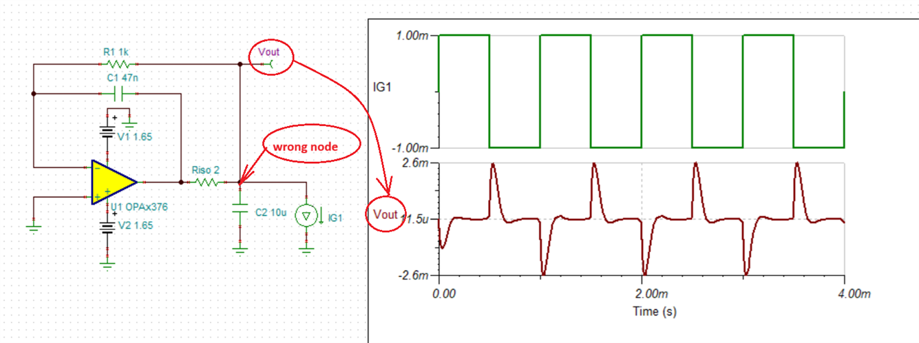
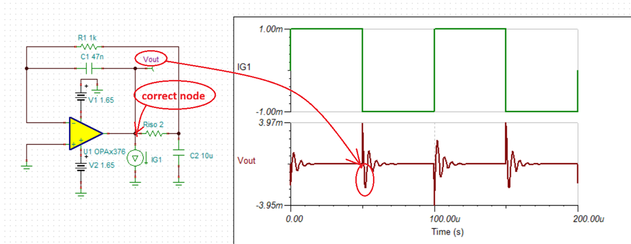
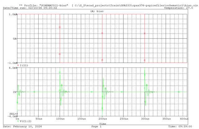
Transient stability analysis must be determined by looking for the small-signal overshoot directly at the output of the op amp and NOT on the other side (right side) of isolation resistor - see below. Also, please notice 10x faster response time (100us/div instead of 1ms/div) between two different nodes.
A small-signal overshoot of 58% aligns closely with theoretical value of 22 degrees phase margin - see below.
The stability analysis based on overshoot can ONLY be determined under linear operation (using a small-signal output of 10mV or less.) Using 1V signal as you show below forces the output to slew and results in a non-linear operation, which cannot be used to draw conclusions about stability of the system.
Thanks for the explanation. If the load capacitor is determined, do you have a process to select the proper RISO/RF/CF? Do you have a method to verify the design by simulation(maybe transient overshoot simulation)?
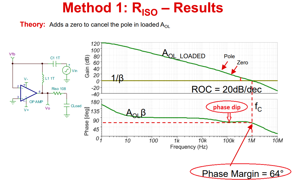
The thread above already shows how to verify stability by simulating phase margin (minimum 45 degrees) and confirming stable operation with small-signal transient analysis (max 25% overshoot). As far as procedure goes, first, you need to determine the minimum Riso value (without dual feedback) by iteration of its value so the phase margin of AOL*Beta (at the intersection of AOL and 1/Beta) is at least 45 degrees while the dip of the phase margin (at any frequency) is above 25 degrees - see below.
Next, you need to add dual feedback initially setting CF=~C2/100 and RF=~Riso*1000 with possible iteration of the component values as needed to meet the overall stability requirements as previously discussed.
For more detailed information regarding circuit stability please review attached presentation.
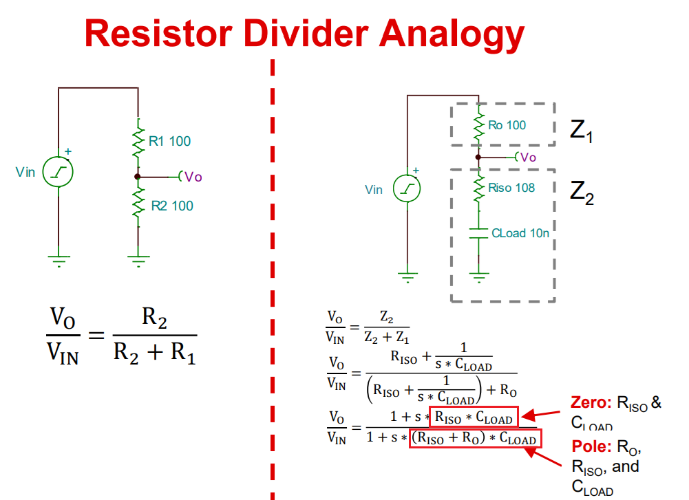
The key point is to understand that there are multiple approaches to solve stability issue. The one I showed above relies on the optimization of phase margin whereas the one you alluded to above places a large cap load at the output (with no Riso) resulting in the creation of second pole at 146.5kHz, which then is used to back calculate the internal output resistance, Ro. Once you know what Ro is, you may use it to choose Riso between Ro/10 and Ro.
Please read the design steps below.
Choosing Riso=Ro will result in the very stable system due cancelling zero occurring within 2x of the pole frequency whereas using Riso=Ro/10 will separate second-pole from cancelling zero by 10x frequency difference (see equations below); however, this may result in an excessive dip in the phase and that's the reason why there is need for iterations to minimize Riso without allowing phase to dip below 25 degrees. - see equations below.
Please note that phase dip is not the same as phase margin. Phase margin is determined at the intersection of AOL and 1/Beta (it's recommended minimum 45 degrees) while phase dip may occur at any lower frequency and requires minimum 25 degrees - see below.
I think I am start to understand your point now. I need to find the second pole which is zero frequency, fp. The first pole is from 0dB/dec to 20dB/dec. And the second pole is from 20dB/dec to 40dB/dec. Then calculate RO. Then for RISO.
And need to verify the phase dip and phase margin based on the RISO selected.
Just a recap: you need to temporarily add a large output cap that will form a second pole (the first pole, around 1Hz above, is the dominant Miller cap inside op amp) and from fp2 frequency back calculate Ro. Using Riso=Ro will assure stable circuit no matter what but if you need to minimize Riso (e.g. because of the output voltage headroom issue) you may go lower than Ro but then need to make sure by iteration of Riso that phase margin (@ frequency where AOL=1/Beta) stays above 45 degrees while phase at any lower frequency doesn't dip below 25 degrees.
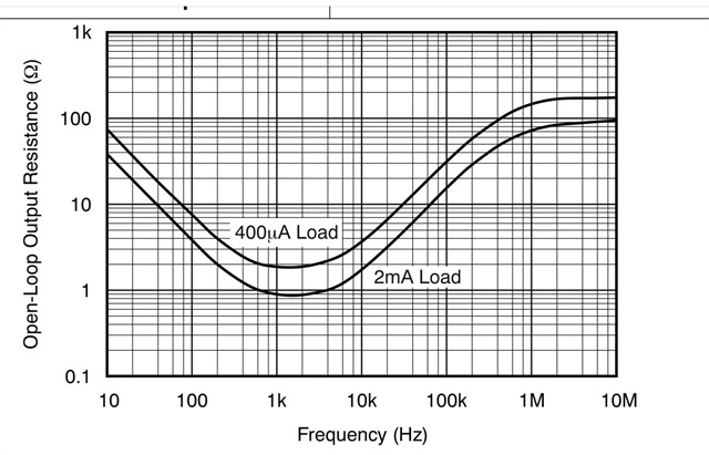
It helps me understand more about the stability. By the way, it seems the output impedance is not always a constant. I see in some datasheet, it varies with the frequency.
Only in op amps using bipolar transistors open-loop output impedance, Zo, is relatively constant over frequency (is resistive - Ro). In all CMOS op amps Zo varies greatly over frequency. For this reason, in order to determine stability of the circuit one must use our simulation macro-models, which meticulously model said variation. Below please see OPA376 Zo vs Frequency graph.
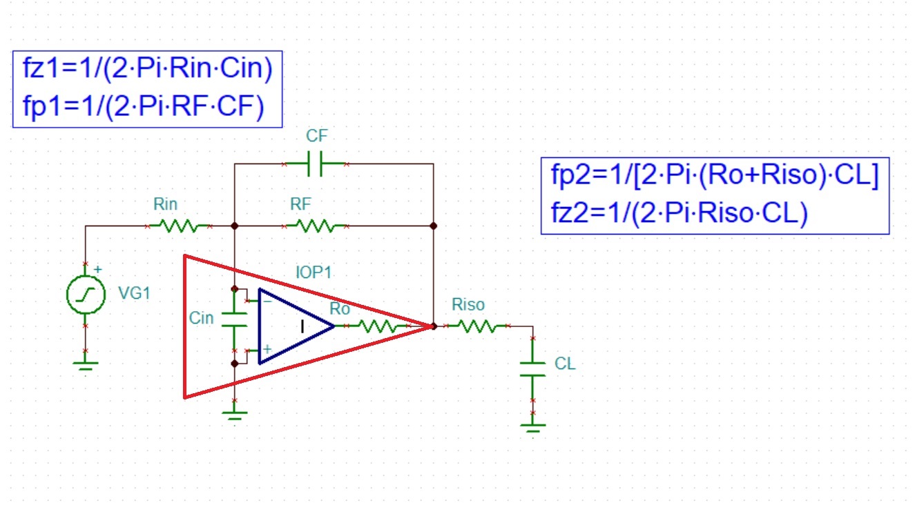
There are two main sources of circuit instability:
1. an interaction of Rin with internal input capacitance (Cin) results in fz1 zero in 1/beta, which should be cancelled with addition of a fp1 pole by adding CF
2. a large capacitive load (CL) will interact with internal output impedance (Ro) forming fp2 pole in AOL, which should be cancelled with introduction of fz2 zero by adding Riso - see below
Could you explain why phase dip should > 25 degree? If it will cause unstable, how it cause the unstable? Because AOL seems fine at the phase dip frequency.