This thread has been locked.

If you have a related question, please click the "Ask a related question" button in the top right corner. The newly created question will be automatically linked to this question.

PGA281: Square Wave and Triangular wave for response for PGA281

Part Number: PGA281
Other Parts Discussed in Thread: PGA855, PGA854

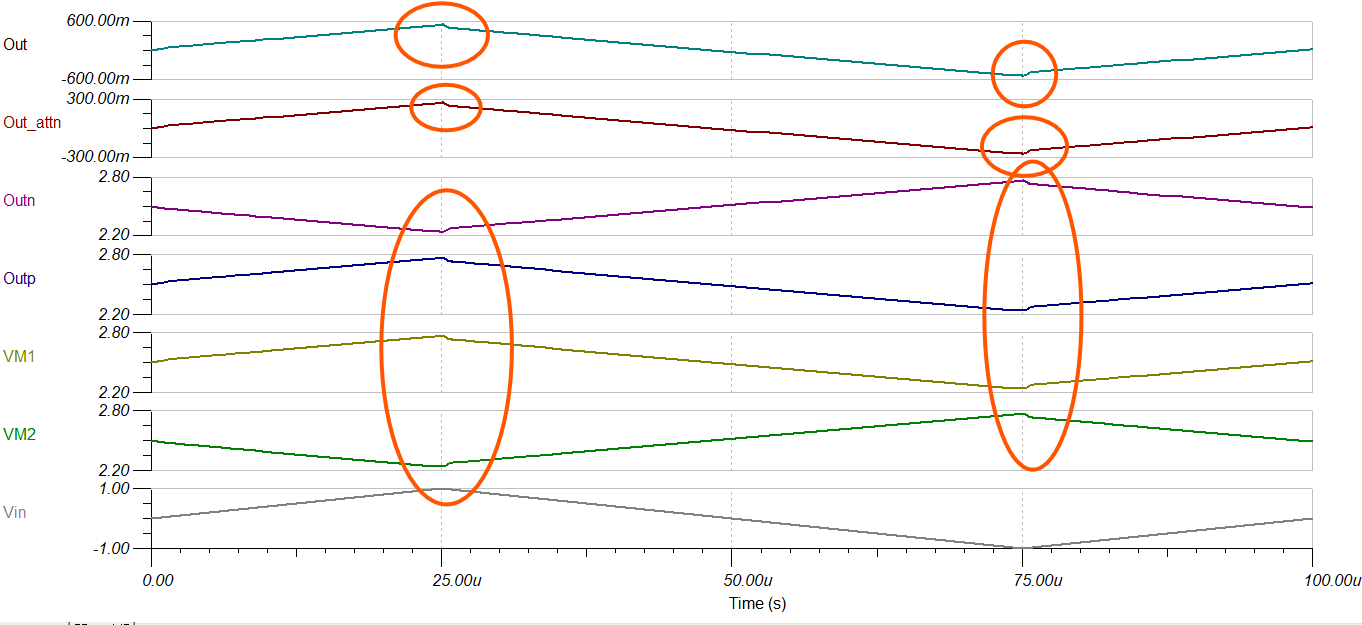
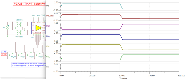
Hi We are using PGA281 in our design, attached the tina simulation and schematics, we want to know why traingular and square wave response has distortion at peak.PGA281_afb23_a1.TSC 
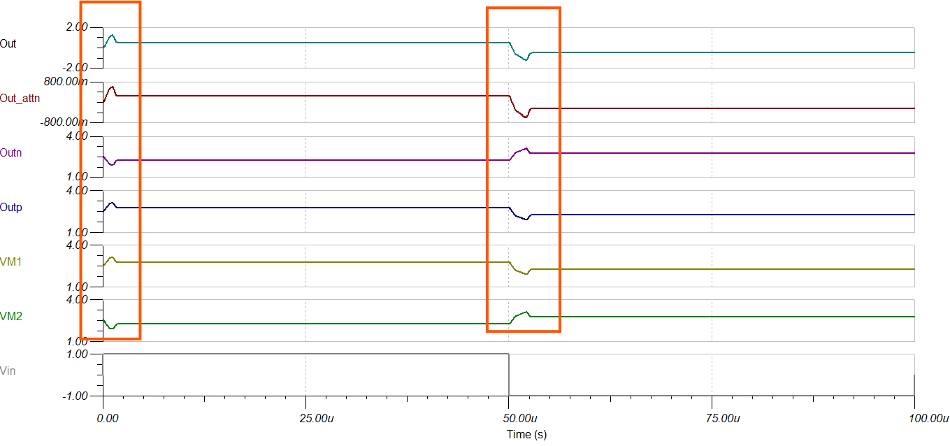
image.png

image.png

  • Hello, 

    I am trying different configurations in the TINA and PSpice to see if I can find the reason for this behavior. I will respond this thread once I have more information. 

    Thank you!
    Regards,
    Ashley

  • Hello, 

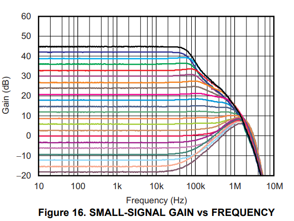
    This behavior is occurring due to the bandwidth limitations at lower gains. Please see figure 16 in the datasheet as shown below.

    I made a few adjustments to the simulation. One is the VCVS blocks were changed to 500mV so that the input signals are just changed differentially but not amplified on the input. 

    When I increased the gain and leaving the input signal the same, the output signal improved. Another way is the modify the input signal. The PGA281 is optimized for low frequency, slow moving input signals. 

    Gain = 1

    Gain = 2

    Please let me know if you have further questions.
    Thank you!

    Best regards,
    Ashley

  • thanks , Any better PGA which will work for us with lower gains?

  • Hello, 

    The PGA855 and PGA854 should be better fits for this, since both parts have better performance across frequency.

    The PGA855 is offered with the following gains: 0.125, 0.25, 0.5, 1, 2, 4, 8, and 16
    The PGA854 is offered with the following gains: 0.5, 1, 2, 5, 10, 20, 50, and 100

    I saw in the simulation that the gain of interest is 0.25, which is served by PGA855. Is the maximum gain of 16V/V compatible to your application? Or is the max gain (176V/V) of the PGA281 required?

    We unfortunately do not have a super robust model on the web right now for the PGA855. However, I can test this on the PGA855EVM Evaluation board | TI.com for you as needed. 

    Would an initial test to see how the PGA855 responds to an input changing from 1 to -1V over the course of 25us in a gain 0.25V/V with power supplies of ±12V for the input stage and single supply 5V on the output stage be sufficient? 
    If not, please specify test parameters. 

    All the best,
    Carolina

  • Hello Chandra, 

    Thank you for the details, I will now remove the post to protect your IP. 

    I will test this in lab comparing the performance of the PGA281 and the PGA855 and reply back in this thread. Expect a response by Friday, EOD, US CST. 

    All the best,
    Carolina

  • Hello, 

    I only have the PGA855 data right now, I will provide the PGA281 data by end of day Tuesday. 
    For all these charts, test conditions are as follows: VS = ±12V, LVDD = 5V, LVSS = GND, VOCM = 2.5V, Gain is 0.125V/V. 

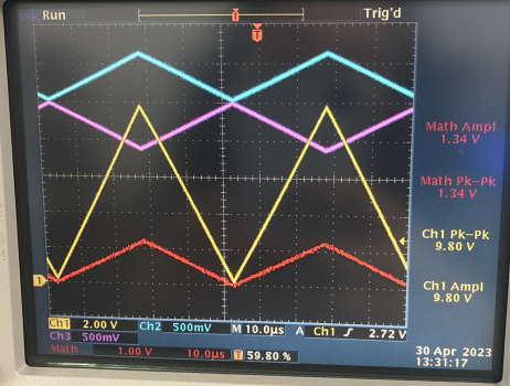
    For a precise 7Vpp input the expected output is 875mV, I am not using a precision signal generator - therefore assume error in PGA855 is minor (equipment used is at fault for inaccuracies). I see around 950mV in my imprecise equipment. 

    I also tested a larger 10Vpp input, this is the max the signal generator can provide, expected output is 1.25V. I see around 1.34V in my imprecise equipment. 

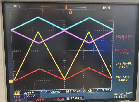
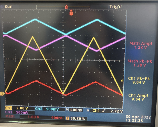
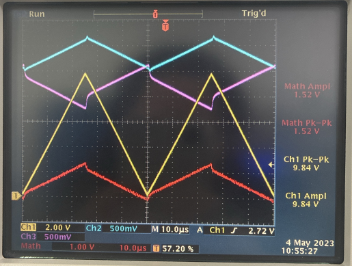
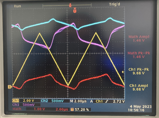
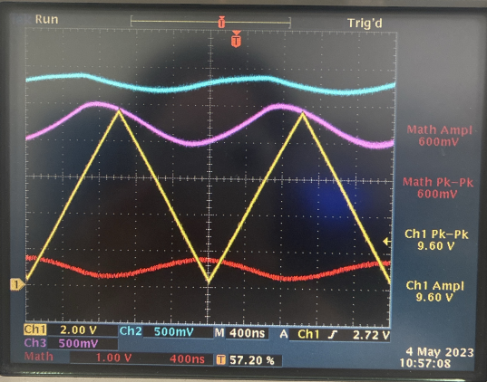
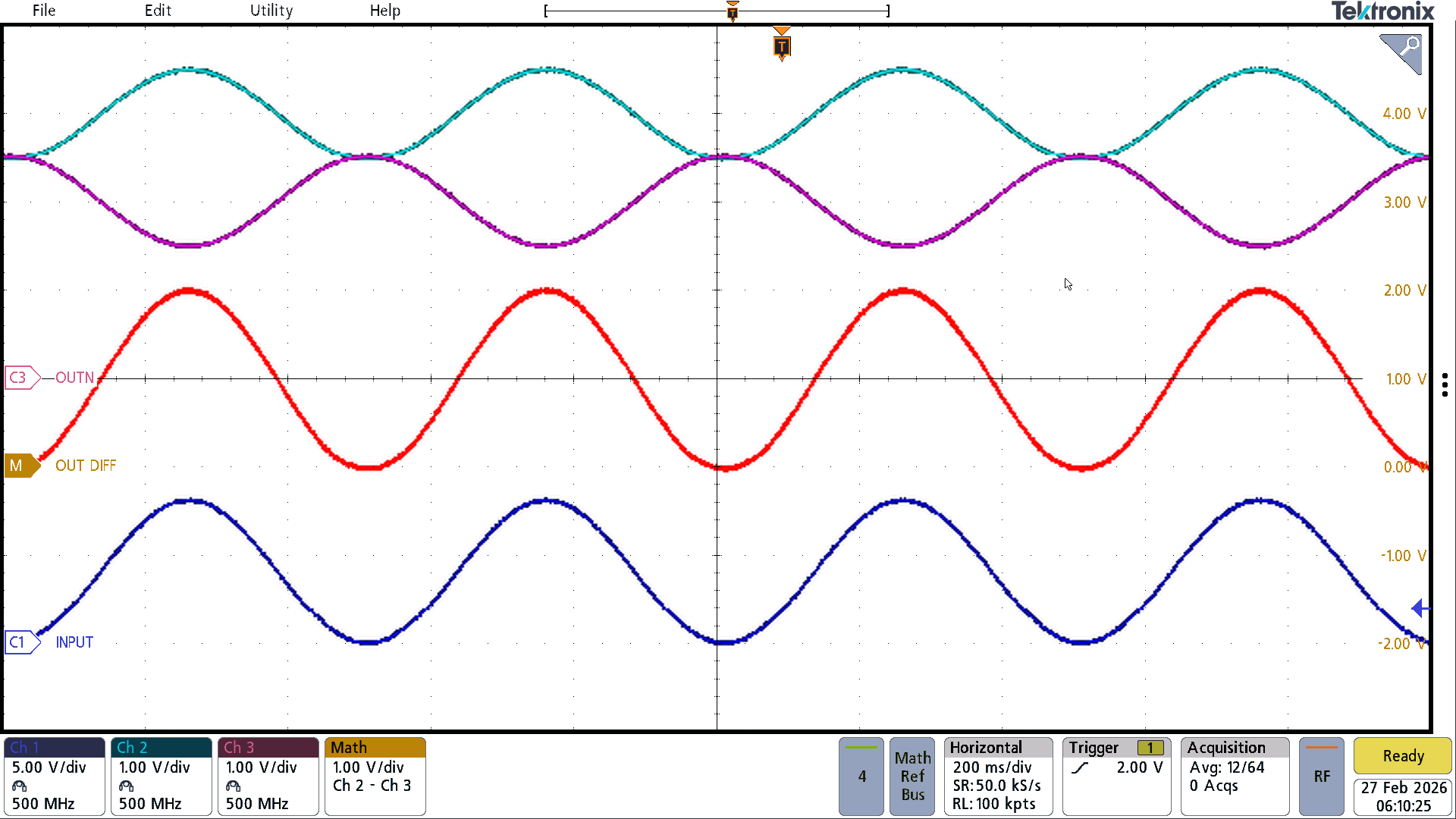
    The input is the CH1 (yellow), OUT+ is CH2 (blue), OUT- is CH3 (pink), the Math channel (red) is CH2-CH3 (difference between OUT+ and OUT-). 

    For 7V input with a 25us rise time, the PGA855 provides an expected output

    For 10V input with a 25us rise time, the PGA855 provides an expected output

    For 10V input with a 5us rise time, the PGA855 provides an expected output

    For 10V input with a 1us rise time, the PGA855 provides an output that is being slightly reduced

    All the best,
    Carolina

  • Hello, 

    As a follow-up, here is the PGA281 performance in the same conditions. 

    7V, 25us rise time

    10V, 25us rise time

    10V, 5us rise time

    10V, 1us rise time

    My recommendation is to go forward with the PGA855 instead of PGA281. 

    All the best,
    Carolina

  • Hi Thanks for sharing Triangular wave results appreciated the efforts been spend on explaining the issue with PGA281. We need same graphs for Sinusoidal and Square wave too to compare PFA281 and PGA855. Also could you check in provided schematics(Deleted IP) what we doing, any thing wrong with respect to capture ADC data. 

    No problem:

    Problem 1:

    Problem 2:

  • Hi, 

    Okay I see, I think the problem has something to do with the DAC power supply (AVDD is 3.3V). 
    Could you please attach your schematic again? I don't remember there being a DAC on it.

    All the best,
    Carolina

  • Hi Carolina,

    Currently what we need to validate is as below only,

    our interest is with gain of 0.125/0.25 given input at PGA281 and what is the output at PGA281 and What we get output at LTC1566-1IS8#PBF(Antialiasing filter).

    Here is the circuit,

    The DAC results what is shared you can Ignore those are coming after FPGA, they are for our internal purpose to validate the input signals.

    ADC --> FPGA --> DAC 

    Rgds

    Chandra

  • Hi, 

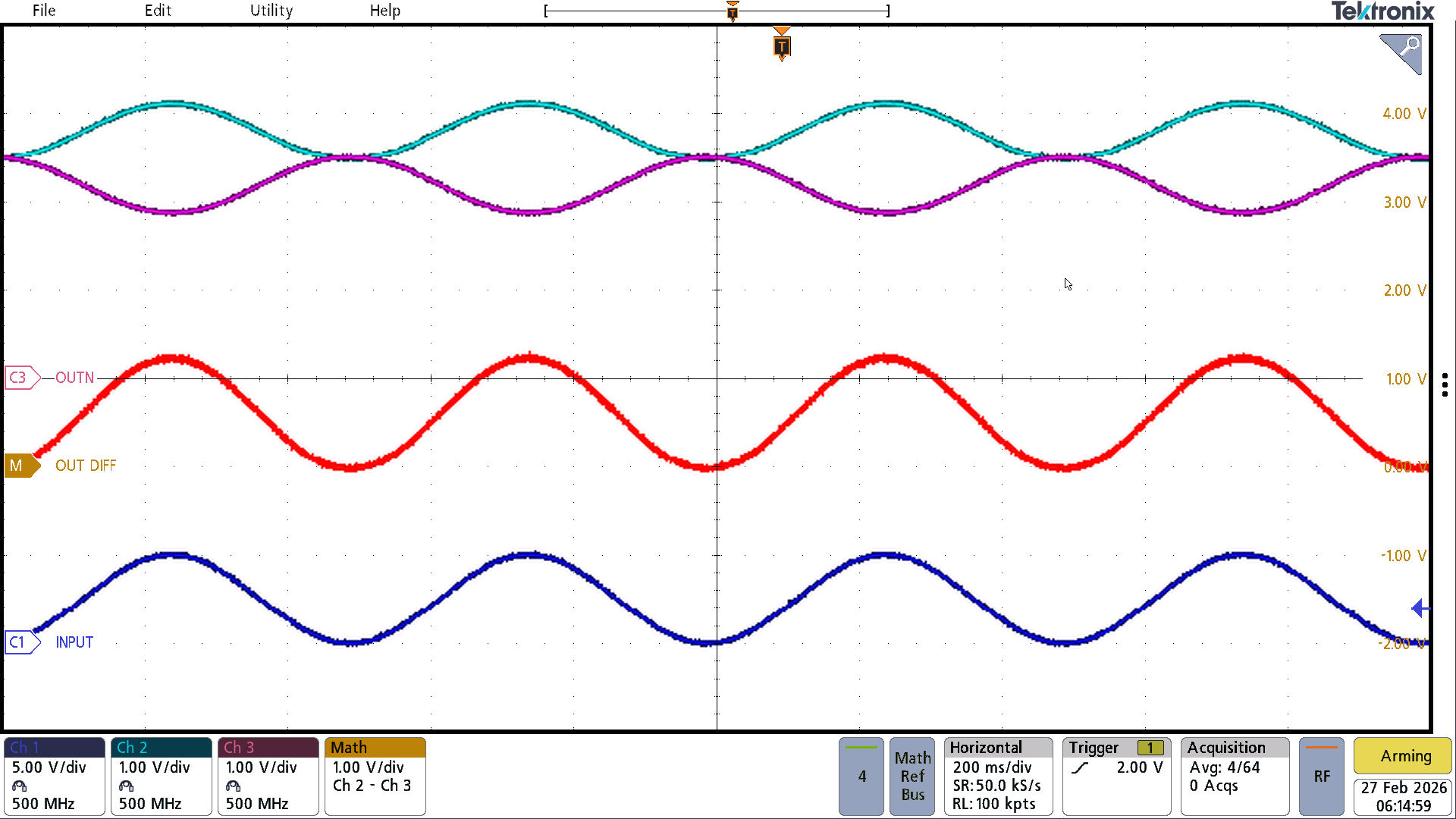
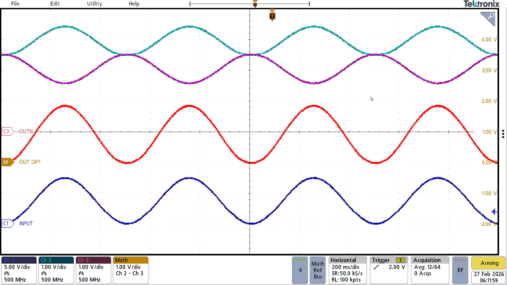
    Thank you for attaching the schematics again, could you please let me know if the input signal is 2Hz? 

    From counting the divisions in the oscilloscope capture, a period is 500ms. Therefore, if we calculate for frequency = 1/500ms = 2Hz. 

    All the best,
    Carolina

  • Hi, 

    That is very slow moving, therefore I don't expect it to be a bandwidth/slew rate issue (as the ramp wave was). 

    I will take steps to see if I can recreate on my end. 
    It looks more like the instrumentation amplifier is limited due to a supply voltage. 

    I am on holiday right now until 2/24 - I will have more test results on 2/26. 

    All the best,
    Carolina

  • Hi, 

    Thank you for your patience, here is the data for the PGA281 (with the conditions outlined above). 

    Input signal (2Hz sine) Input common mode  Input differential PGA281
    5Vpp 2.5V 2.5V
    7.4Vpp 3.7V 3.7V
    8Vpp 4V 4V

    As you can see, I am not able to replicate the test results on the EVM. I think the problem is the voltage on VSOP (pin 9) and VSON (pin 12) on the PGA281. Please double check this voltage in the testing. 

    All the best,
    Carolina

  • Hi Carolina,

    Thanks for your scope shots,

    It seems we identified the issue who us causing the problem but still why this is problem we are not sure, Here below experiment we did,

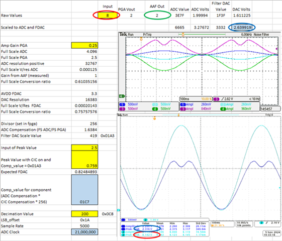
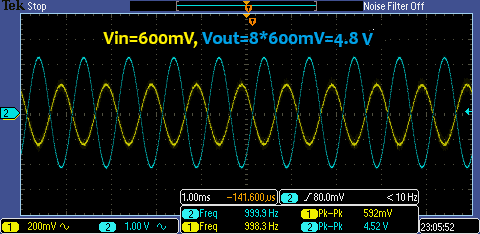
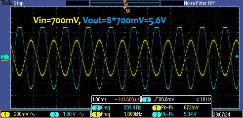
    This is the input of PGA and Output of the PGA with gain of 8. PGA seems working proper.

    Any thing above 5V will starts clipping as expected VSOP is 5V in our case.

    Now real problem after Antialiasing filter,

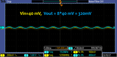
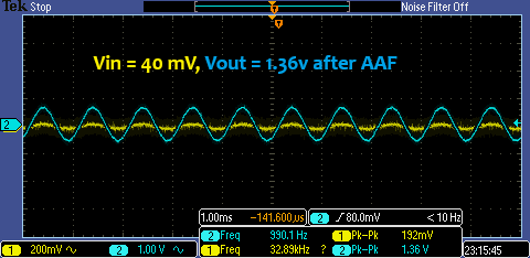
    This is the capture at input of PGA and output of PGA for 40mV input.

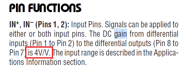
    This is the capture at input of PGA and output of Antialiasing filter(AAF). We have gain 4V/4 that is why do we have amplified signal at AAF output. But why it clips for >1.65V at AAF output?

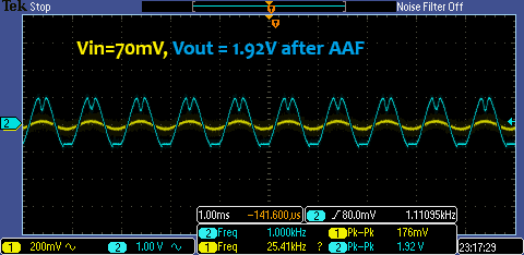
    If you see below anything more than 70mV, we start clipping at AAF output, refer below.

    We see here it started clipping >1.65V output. Are we missing anything here.

    My Oscilloscope having less resolution so ignore the CH1 reading measurements for Lower voltages(40mV, 70mV). 

    our application is DC coupled input.

  • Hi, 

    Looks like you are running into a headroom limitation based on power supply. I am not familiar with the device and cannot provide support as it is not a TI device. I can say that the waveforms you are showing look a lot like phase reversal seen in op amps - which occurs when the output is above the allowed voltages - due to power supply. 

    Please let me know if there are additional questions regarding the PGA281. 

    All the best,
    Carolina

  • Dear Carolina,

    We found the problem, it seems Anti aliasing filter what we using was the problem,

    It need -V to be connected with negative 5Volts to support 2.5Vpp. We are happy to close this as resolved. Thank you so much for your support.

    Rgds

    Chandra

  • Hi Carolina,

    Since you have an evaluation board can you please do us favour, since we decided to to go with PGA855 for next version of PCBs, we want to capture few graphs for 50Khz, 100Khz, 250Khz, 500Khz, 1Mhz, sinusoidal, Square wave and Triangular wave will you be able to help with this data for all voltages as we did earlier.

    Thank you so much in advance.

    Rgds

    Chandra

  • Hi Chandra, 

    To align, the test conditions are as follows: VS = ±12V, LVDD = 5V, LVSS = GND, VOCM = 2.5V, G = 0.125 V/V 

    Input (single ended), IN- = GND. IN+

    Voltage level: 5 Vpp, 7.4 Vpp, 8 Vpp, 10 Vpp

    Frequency: 50 kHz, 100 kHz, 250 kHz, 500 kHz, 1 MHz. 

    Shape: Sine, Square, Triangular 

    This is a total of 72 tests. Since I am doing this by hand, I will reduce the test list to the following:

    Voltage level: 5 Vpp, 7.4 Vpp, 8 Vpp, 10 Vpp

    Frequency: 50 kHz, 100 kHz, 250 kHz, 500 kHz, 1 MHz

    Shape: Sine, Square, Triangular 

    This is the total of 18 tests - much more doable in a reasonable time frame. If you need all 72 tests done or need a different selection of 18 tests, please let me know and I will adjust accordingly. 

    I can have these tests done by April 10th, EOD Dallas Time. 

    All the best,
    Carolina

  • Hi Carolina,

    Thanks yes I agree with you. appreciated your quick response.

    Rgds

    Chandra

  • Hello, 

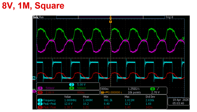
    Please see results attached, the 10V input voltage level didn't work as well as I had hoped at fast frequencies. Please let me know if you would find it helpful to see it at 8Vpp. 

    PGA855 Single-ended performance.pptx

    All the best,
    Carolina

  • Hi Carolina,

    Thank you so much for your waveforms these details, We did analysis the plots. Can you please add up the plots also with 8Vpp. 

  • Hi Chandra, 

    Great to hear, I will have these done by Monday, EOD. 

    All the best,
    Carolina 

  • Hi Chandra, 

    Please see the measurements attached. 

    PGA855 Single-ended performance_v1.0.PPTX

    All the best,
    Carolina

  • Thanks Carolina,

    This helped us a lot, 

    Need few clarifications of faster raise time response of PG855, Why do we see such behavior? Is it raise time is too fast for PG855? Can me adjust the raise time and test with 8V/10V, We wuld like to know for 1Mhz signal what could be raise time acceptable by PG855. Any input capacitance limiting our fast raise time?

    Rgds

    Chandra

  • Hi Chandra, 

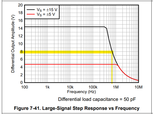
    I think the limitation is internal to the device. If we consider Figure 7-41 from the datasheet, we see the full power bandwidth response from the output of the PGA855, by definition this is done with a sine wave. 

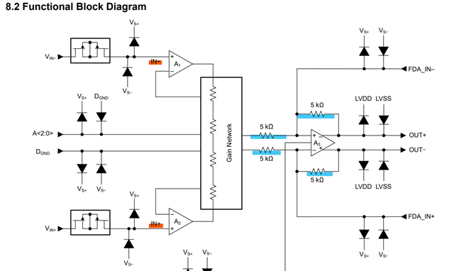
    If we look at the block diagram of the PGA855, the output stage is in a gain of 1 (see blue), and the input stage is in a non-inverting gain, whose gain equation is 1 + RF/RIN (see orange). 

    Although we cannot see what is in the gain network, we do know the minimum gain on the input stage is 1. The attenuation therefore occurs somewhere in the middle box (labeled gain network). 

    Assuming everything is in a gain of 1, the 8V input signal is bandwidth limited around 700kHz. As I mentioned earlier, this graph is for a sine wave, depending on process variation (the bandwidth can shift 30%), input signal, balanced inputs - I think it most apparent in the square wave but to any extent it is a device internal limitation. 

    All the best,
    Carolina 

  • Thanks Carolina, You have done good job to support us on this. Appreciated the efforts and feedbacks. I got all details what is required. In case of any more details will write back. 

    Thanks

    Chandra

  • Wonderful, great to hear!