This thread has been locked.

If you have a related question, please click the "Ask a related question" button in the top right corner. The newly created question will be automatically linked to this question.

TAS6424E-Q1: Behavior at low temperature(-40 degree)

Part Number: TAS6424E-Q1
Other Parts Discussed in Thread: TAS6424E,

Hi,

We are currently facing an issue that is blocking our ongoing evaluation, so I would appreciate your urgent support on this matter.

Symptom

  • Channel 2 of TAS6424E does not play at a temperature of −40°C.
  • Under this condition, we measured the DC voltage at OUT_2P and OUT_2M and found that only 2.4 V is present after the LC filter.
    At the same time, OUT_3P and OUT_3M output approximately 6 V, and a sine wave is played normally.

Test Conditions

  • Temperature: −40°C
  • Supply voltage: 12 VDC
  • Speaker output setting:
    • CH1 and CH4 are muted
    • CH2 and CH3 are enabled (state = Play)
  • SAP Control (0x03): 0x44
  • Speaker output level: 1 Vrms for each channel

This issue is preventing us from proceeding with further evaluation.
If possible, we would appreciate it if you could share any initial feedback or considerations by tomorrow, even if it is a preliminary opinion.

Thank you in advance for your support on this urgent matter.

Best regards,

  • Hi Yusuke,

    Are you using PPC3 or your own MCU? If using PPC3 could you please provide the fault flag that you see? If you are using your own MCU, could you please read register 0x10-0x13?

    Another thing is how are you reading the -40degC temperature? It might not be an accurate representation of the temperature. How long have you been playing? The abs max rating of TAS6424E-Q1 is -55degC to 155degC, if your temperature is not accurate and you have been playing in that temperature for a while, it might damage the device.

    Regards,

    Leo

  • Hi Leo san,

    Thank you for your quick response,
    And I will answer to you 1 by 1,

    1. Are you using PPC3 or your own MCU?
        this is own MCU, so that I will try to read those register.

    2. how are you reading the -40degC temperature?
        we use the calibrated thermostatic chamber and make the temperature to -40degC.
        and of course this chamber cannot make below temperature more than -55degC, so that your guess might be not correct.

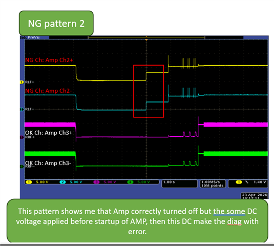
    And I found interesting waveform at start up diag,
    Could you please check the attached document and investigate how can TAS6424E can output such diag waveform?
    Behavior at low temperature(-40degC).pptx

    And also attach the flow of DC diag when startup,
    so if you have comment please let us know.
    Diag flow at startup.xlsx


    Best regards.

    Torikai

  • Hi Torikai-san

    I checked customer's waveform. The abnormal situation, DC load diagnostic not able to pass. Please get the register value at 0x0C and 0x0D, to check which of the fault been detected. 

    It is possible some kind of shortage happened at the low temperature situation.

    The IC itself, is not much concern for this using condition. -40C is one of our side validation test environment. 

  • Shadow san

    Thank you for your confirmation,
    I will continuously trying to read the value(currently we don't have way of checking the value directly so under preparing, sorry for wait)

    And I found additional symptom based on my waveform and newly taken.

    So could you please suggest me for this symptom?
    Behavior at low temperature(-40degC)_Add0423.pptx

    Best regards.
    Torikai

  • Hi Torikai-san

    Quite strange about their waveform. I'm not fully sure it's the IC output them directly, or any external soft shortage. At below picture, when the output CH2 has a voltage jump, did customer send out any I2C command or not?

    And from their test results, the problem always on CH2. Is the problem only happens to this specific IC, and also specific channel 2? 

    Could customer try some ABA swap test, to see if the problem follows the IC, or follows the PCB?

  • Dear Shadow san,

    Thank you for your confirmation, 
    And until today I checked this symptom under -40degree,
    And this DC is output from TAS6424E, as you can see in below.
    So I will continue to check, so could you please confirm the estimated mechanism of this DC from structure point of view?


    And we found 2 other symptom,
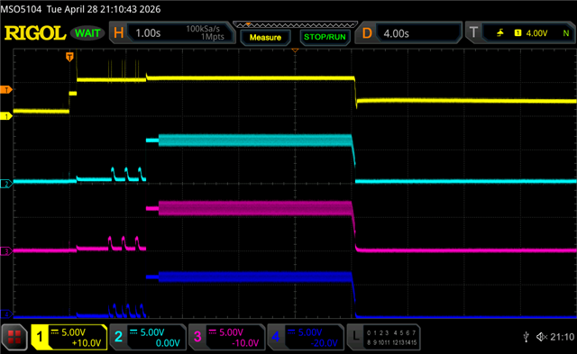
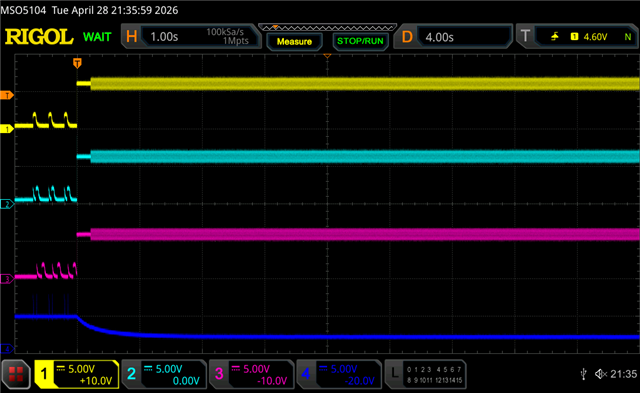
    1. shutdown waveform depends on temperature.
    this shutdown waveform depends on the temperature as I showed in below 2 picuters.
    Yellow Ch2
    Light Blue Ch3
    *please ignore pink and blue waveform

    Under 25 degree


    Under -40 degree


    2. another not operated ch
    there is another trigger that the Amp ch no sound like below.
    Do you have any estimation?
    The dark blue waveform is the ch not have output.
    It looks not output any switching.


    Best regards.
    Torikai

  • Hi Torikai

    The waveform is quite abnormal and can't be explained. I checked with our validation team, that also doesn't have the similar record before.

    The most important thing, is to make clear this abnormal waveform coming from silicon itself, or external shortage. Especially they having some continuous bias voltage at around 2.5V on the waveform.

    Any chance they could remove 1 of the channel's inductor on the PCB? Choose the channel that easy to reproduce this issue (maybe the yellow one, or dark blue), remove both OUTN and OUTP. And test the waveform close to the silicon side. If still could find out such waveform, we'll able to confirm the problem is the silicon alone.

    And if it is indeed from silicon, we need to check if this single silicon having problem, or they has multiple IC facing the same issues. 

    Thanks.

  • Hi Shadow san,

    I found an incorrect understanding regarding how VDD should be handled after the STANDBY pin is deasserted.
    Therefore, I would like to understand the mechanism behind why VDD must not be pulled low within 15 ms after the STANDBY pin is deasserted.
    Could you please provide some insight into this behavior and also comment on whether this consideration is reasonable for addressing the first issue?

    OperationVoltage_LowTemp_ForTI.pptx


    Best regards
    Torikai

  • Hi Torikai san

    Pull low STANDBY pin, IC would start to going into shutdown process. It needs several ms time, because IC would need to slowly ramp down the output to avoid pop noise. The process is major controlled by the digital logic, which powered by VDD supply. If you don't wait 15ms time, the shutdown process would be interrupt, and would create the abnormal waveform. So the first issue should be this root cause.