Part Number: THS4551
Other Parts Discussed in Thread: TINA-TI, ADS5281, LMH6553, THS4541, ADC3910D125, OPA188, DAC80504, OPA227
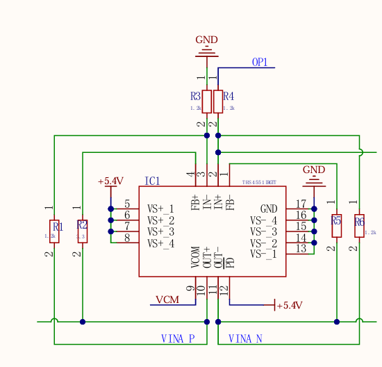
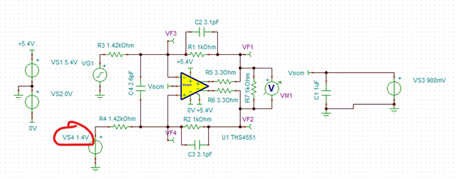
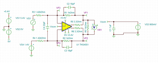
I am using the THS4551IRGTT (16-pin VQFN package) as a fully differential amplifier to drive an AD9257 ADC. The ADC operates with AVDD = 1.8 V and provides a VCM of 0.9 V (AVDD/2), which is connected to the THS4551 VOCM pin. The THS4551 is powered from a single 5.4 V supply.
My resistor values are R1 = R3 = R4 = R6 = 1.2 kOhm and R2 = R5 = 3.3 Ohm in a single-ended to differential configuration. The input signal is a single-ended analog signal with a maximum amplitude of 2.8 V peak. I would like to keep the THS4551 differential output below 1.8 Vpp to avoid overdriving the AD9257 inputs.
Could you please confirm whether this resistor configuration is appropriate, or whether the THS4551 output will saturate with this input signal level?
I would also like to understand the role of the FB+ and FB- pins in this configuration and how they affect gain setting and FDA operation.
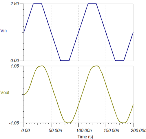
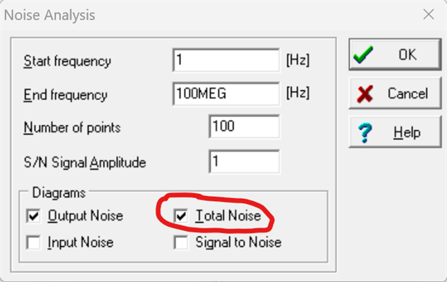
In addition, I would appreciate guidance on how to verify the design using TINA-TI or PSpice. Which simulations should be performed to confirm that the output common-mode voltage remains at 0.9 V, the amplifier operates linearly without clipping, and the differential output swing remains within the ADC input range?
Is transient analysis of OUT+, OUT-, and the differential output (OUT+ minus OUT-) sufficient, or are there other recommended simulations or measurements?
Finally, is it practical to validate this design on hardware using an evaluation board or prototype setup before committing to a PCB design?