OPA192-Q1: Attenuation and stability

Part Number: OPA192-Q1
Other Parts Discussed in Thread: OPA192, OPA209, , OPA994-Q1, OPA994, OPA2994, OPA2994-Q1

OPA192 is used in the circuit to make from 5V to 6V but there is voltage drop AT 6V output of Opam for the load current of 20mA why this happening. And if i go near to OPA192 Supply single ended 7.5V there is no drop what does this mean?  OPA192 Single ended supply 6.5V image.pngIC 16 is OPA192 with capacitors of 0.1uF and 10uF ,
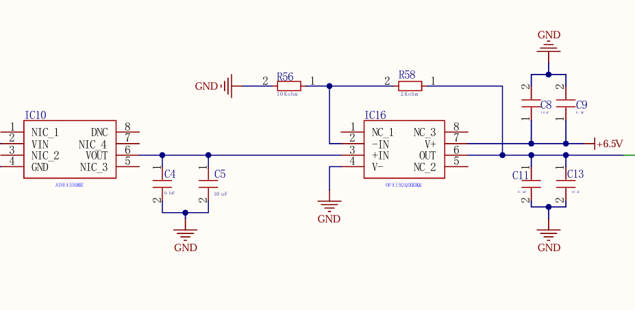
ADR4550-RZ referenece IC of 5V having output CAP of 0.1uF,10uF 


I have a precision 5 V reference available at the IN+ input, and I need to generate an adjustable output range of 6V from this reference.

I would like to achieve this with very good accuracy and stability. Could you please recommend the appropriate op-amp configuration and resistor network to scale the 5 V reference to a 0–1.5 V output? for same type of circuit  <0.25mV stability 


Could you please recommend a suitable TI precision op amp and the recommended circuit topology for converting the 5 V reference to a precise 0–1.5V adjustable output?

  • Nishant,

    • The OPA192 is a good choice for driving a capacitive load.  It has a Zo property that is specifically designed to help drive capacitive load.  However, it does require some external components to make the circuit stable.  There are some "unlimited capacitive drive op amps", but these are generally not precision devices.  Furthermore, even though the unlimited cap drive devices are stable they will loose phase margin for some capacitive loads.  Basically, these devices will not oscillate across a wide range of capacitive load, but they will have overshoot and ringing (i.e. loss of phase margin).
    • Below is a circuit that will be stable for you gain and output capacitive load requirements. I did an open-loop and closed loop test.
    • The methods used to design and test the circuit are documented in Operational Amplifier Stability Theory and Compensation 

    opa192 ref drive open loop.TSC

    opa192 ref drive trans.TSC

    Best regards, Art

  • I am not having bipolar supply. I have single ended supply that is 6.5V or 7.5V . So please tell  for that . And I have to maintain stability of 0.25mV in the output voltage that is 6V or 1.5V or 1V  so how to do that in one case i need to attenuate from 5V reference IC to 1V or 1.5V and in one case i need to do amplify from 5V to 6V . So please tell how I can maintain that stability in output Voltage and the capacitors at non inverting terminal of amplifier present are of reference iC output voltage 5V 0.1uF and 10uF as written in datasheet of reference IC . Reference IC is used to get good ppm over entire temperature range(-40 to 125degree Celcius) and good stability of less than 0.25mV prevision in voltage . So how to do that

     And output load current required is only 15-20mA so for that amplifier is used to drive that load at that Voltage 

  • Also tell the procedure to check stability of output voltage in Hardware and simulation to verify it is less than 0.25mV . Please tell Hardware setup and measurement method. It will be highly appreciated.Stability is different from output voltage ripple in output Voltage. Please consider that. If I am wrong please correct.but requirement is less than 0.25mV stability typical

    Thanks & Regards 

    Nishant 

  • Hi Nishant, 

    I am not sure we understand the new requirements. Can you modify the Tina file to show us your circuit and conditions? For stability on a single supply the method would be the same as Art showed. I have modified Art's sim to check the phase margin on a single supply of 6.5V. The updated Tina file is attached below. If you can open up the file and modify it to help us better understand your design requirements that would be helpful. 

    5670.opa192 ref drive open loop.TSC

    We have a very detailed video training on stability and testing in simulation using Tina that can be found here:

    https://www.ti.com/video/4080235259001

    Best Regards, 
    Chris Featherstone

  • I am facing an issue with the OPA192 in hardware and would appreciate your guidance on whether I am missing any fundamental limitation related to output voltage headroom or output-drive capability.

    In my circuit, the OPA192 is powered from a single 6.5 V supply (VCC) and is configured to provide approximately 6 V at the output. The required load current is approximately 20 mA.

    However, during hardware testing, the output does not remain stable at the expected 6 V when the 20 mA load is connected.

    My understanding was that the OPA192 has relatively high output-drive capability (up to approximately 60 mA), so I expected it to be capable of driving a 20 mA load. Also, since the device is specified as a rail-to-rail output op amp, I initially assumed that a 500 mV difference between the supply rail and the required output voltage should provide sufficient margin.

    My questions are:

    1. Is the OPA192 actually capable of maintaining a 6 V output while sourcing 20 mA from a 6.5 V single supply?
    2. Does the specified output-drive capability of approximately 60 mA mean that the device can maintain the required output voltage at that current, or is the available output voltage headroom an important limitation?
    3. In this configuration, is the 500 mV headroom between VCC = 6.5 V and VOUT = 6 V insufficient for the required 20 mA load?
    4. Are there any specific VOUT vs. IO / output-voltage headroom specifications or test conditions in the datasheet that I should use to verify this operating point?
    5. Could the observed behavior be caused by the output transistor approaching its voltage headroom/current limit rather than the OPA192 simply being unable to supply 20 mA?
    6. Is there any other fundamental consideration that I may be missing in the basic op-amp operation when using a single supply with the output this close to the positive rail?

    The schematic used for the hardware test is the same as the schematic I have shared; no changes were made between the schematic and the hardware implementation.

    I would appreciate it if you could help me identify whether this is an output-drive limitation, output-voltage headroom limitation, stability issue, or some other limitation of the OPA192.

    Thank you.

  • Nishant,  

    • You cannot achieve a 0.5V swing-to-the-rail on OPA192 with and output current of 20mA.  The best way to understand the typical saturation of the output swing is with the "Output voltage swing vs Output current" curve.  The current released version of the OPA192 data sheet only show swing to the negative supply (figure 20).  The swing to the positive supply curve was lost in a data sheet update.  I have access to the old data sheets and below is an image of both the positive and negative swing.  The positive and negative swing are symmetrical. I will request a data sheet update.
    • The typical swing to the supply rail is 1V for a 20mA output current.  This is just a typical number so the worst case could be worse.  Nevertheless, your circuit needs a swing of better than 0.5V and the OPA192 typical swing is 1.0V, so the OPA192 will not meet this requirement.
    • In general, CMOS devices like OPA192 have excellent swing to the rail for low current and degraded swing for high output current.  Conversely, a rail-to-rail bipolar has about 0.2V swing to the rail over a wide current range.  The OPA209 is a bipolar device that should meet your swing requirements.
    • The "output swing vs output current" curve is discussed in this short article:  The Insidious Claw Curve .  A much more detailed white paper on this topic is in Op Amp Input and Output Swing Limitations 

    Best regards, Art

  • Hello Art Kay,

    I would like to clarify the output-drive capability and stability of the OPA192-Q1 for my application.

    If I use a single-ended 7.5 V supply for the OPA192-Q1, can it reliably generate a 6 V output while driving a maximum load current of approximately 20 mA? The input voltage applied to the amplifier will be 5 V using reference IC as stability is the major concern.

    If the OPA192-Q1 cannot provide 6 V at 20 mA with sufficient output-voltage headroom, could you please suggest a suitable AEC-Q100 / Q1-qualified alternative that can meet these requirements?

    If the OPA192-Q1 can support this operating condition, I would also appreciate confirmation of how much output current it can drive at a 6 V output while maintaining the required output accuracy and stability.

    Another important requirement for my application is that I would like to remove the capacitor currently connected at the amplifier output, as shown in the schematic I shared above. Could you please confirm whether the OPA192-Q1 can remain stable and operate correctly without this output capacitor while driving the approximately 20 mA load?

    For the output-voltage stability requirement, I need approximately ±50 mV output variation for a ±50 mV variation in the supply voltage. The required supply-to-output sensitivity is approximately:

    ΔVOUT / ΔVDD = 0.088 V/V

    Therefore, I would appreciate your guidance on whether the OPA192-Q1 can meet the following conditions:

    • Supply voltage: 7.5 V single-ended

    • Input voltage: 5 V

    • Required output voltage: 6 V

    • Maximum load current: ~20 mA

    • Output capacitor: Preferably removed (Input capcitor also need to remove ? As these are the output capacitor for reference IC which generate 5V precision reference voltage so what to do)

    • Required supply-to-output sensitivity: 0.088 V/V

    • Output variation requirement: approximately ±50 mV

    The OPA192-Q1 is a very good precision amplifier for this application, and I would prefer to continue using it if it can meet these requirements. I would therefore greatly appreciate your confirmation of the output-drive capability, required output headroom, and stability without the output capacitor.

    Thank you for your support and for helping me understand the capability of this excellent amplifier.

    Best regards,
    Nishant

  • Nishant,

    Question:  If I use a single-ended 7.5 V supply for the OPA192-Q1, can it reliably generate a 6 V output while driving a maximum load current of approximately 20 mA? The input voltage applied to the amplifier will be 5 V using reference IC as stability is the major concern.

    Answer:  The typical swing to the rail is about 1V for a 20mA output current (see curve in my previous post).  The key term here is typical.  The worst case swing will be worse than the typical value.  You have about 1.5V from your expected output to your supply voltage.  This give you a little margin.  You need to consider if you have enough margin.  I think it is pretty close and would try and find an alternative.  

    Question: If the OPA192-Q1 cannot provide 6 V at 20 mA with sufficient output-voltage headroom, could you please suggest a suitable AEC-Q100 / Q1-qualified alternative that can meet these requirements?

    Answer:  The OPA192 is a precision op amp.  That means that it has low Vos, low IB, and low noise.  The OPA994-Q1 is a good bipolar device that has better swing to the rail at 20mA.  The OPA994 is not a precision device, so it has VOS and IB that is higher than OPA192.  Since you are creating a regulator I think that the Vos may not be the most critical.  In general, CMOS devices swing to the supply rail will degrade worse than rail-to-rail bipolar for higher current loads.  Also, the OPA994 is designed to be stable versus capacitive load which should help for your applicating.   Another alternative would be to use the OPA192 with a discrete BJT output buffer as shown below.  The nice thing about this approach is that you will still get the DC precision of the OPA192.  Another benefit is that the power dissipation is mostly in the output transistor, so you don't have to worry as much about the op amp self heating.  The output swing should be about 0.7V from the supply rail (use 1V for margin).  Alternatively the output transistor could be a MOSFET.

    Question: If the OPA192-Q1 can support this operating condition, I would also appreciate confirmation of how much output current it can drive at a 6 V output while maintaining the required output accuracy and stability.

    Answer:  I think the OPA192 is marginal for your application.  

    Question: Another important requirement for my application is that I would like to remove the capacitor currently connected at the amplifier output, as shown in the schematic I shared above. Could you please confirm whether the OPA192-Q1 can remain stable and operate correctly without this output capacitor while driving the approximately 20 mA load?

    Answer:  The OPA994 is specifically designed to drive capacitive load.  If you choose this device, please post your intended schematic and I can test the phase margin for you.

    Question: For the output-voltage stability requirement, I need approximately ±50 mV output variation for a ±50 mV variation in the supply voltage. The required supply-to-output sensitivity is approximately:

    ΔVOUT / ΔVDD = 0.088 V/V

    Therefore, I would appreciate your guidance on whether the OPA192-Q1 can meet the following conditions:

    • Supply voltage: 7.5 V single-ended

    • Input voltage: 5 V

    • Required output voltage: 6 V

    • Maximum load current: ~20 mA

    • Output capacitor: Preferably removed (Input capcitor also need to remove ? As these are the output capacitor for reference IC which generate 5V precision reference voltage so what to do)

    • Required supply-to-output sensitivity: 0.088 V/V

    • Output variation requirement: approximately ±50 mV

    Answer: I will do this analysis once you decide:  1) use OPA994, or 2) OPA192 with discrete output transistor.  If you choose OPA192 with output transistor provide me the automotive qualified transistor you want to use.  The main thing to look for is a good current gain (beta or hfe) of 100A/A or better.  You also do not want to use a Darlington because the VBE drop will be too high.  Confirm that the VBE drop is about 0.7V.

    Sorry this is taking a while to resolve.  I think we are close now.

    Best regards, Art 

  • Hello Art,

    Thank you for your detailed explanations and for suggesting the OPA994-Q1 as an alternative to the OPA192-Q1. I appreciate your patience and support in helping me resolve these design concerns.

    Based on your recommendations, I would like to proceed with the OPA994-Q1 for the initial analysis of my 6 V output stage, rather than the OPA192-Q1 alone, because of the output-voltage headroom concerns under a 20 mA load. I would also appreciate your guidance on whether the OPA994-Q1 is suitable for my additional low-voltage output requirements.

    I have consolidated my remaining questions below to clarify the requirements and identify the best approach for the application.

    1. Generating a Stable 6 V Output from a 5 V Precision Reference

    My circuit uses a 5 V precision reference IC as the input to an operational amplifier configured with an Rf/Rg feedback network to generate a 6 V output. The amplifier is powered from a single-ended 7.5 V or 6.5 V supply, depending on the implementation, and the maximum required load current is approximately 20 mA.

    My target is to maintain typical output voltage stability of approximately 1 mV. However, during testing with the OPA192-Q1, I observed a significant output variation, with approximately 180 mV peak-to-peak measured at the output.

    Could you please advise on the following?

    • Is the OPA994-Q1 a suitable choice for generating 6 V from a 5 V precision reference while driving a 20 mA load?

    • What could cause the approximately 180 mV peak-to-peak output variation despite using a precision reference IC?

    • What supply-voltage margin would you recommend for maintaining the output voltage under worst-case load conditions?

    • Can the OPA994-Q1 operate reliably without the output capacitor shown in my original schematic while driving this load? If the capacitor is required, what value and configuration would you recommend?

    2. Generating a Stable 1 V Output from the Same 5 V Reference

    I also need a 1 V output derived from the 5 V precision reference, with a target output variation of approximately <0.25 mV and a load current of 2 mA RMS or 5mA (RMS)tell for both current in consideration.

    For this channel, I would like your recommendation on whether the OPA994-Q1, OPA192-Q1, or OPA209 would be the most suitable device.

    Specifically:

    • Can the OPA994-Q1 achieve the required output stability of <0.25 mV when configured to attenuate 5 V to 1 V?

    • Would a precision amplifier such as the OPA192-Q1 or OPA209 be a better choice for this lower-current application?

    • Would a resistor-divider network followed by a voltage buffer be preferable to an amplifier configured with a feedback network?

    • How should I account for amplifier offset voltage, offset drift, resistor tolerance and temperature coefficient, output impedance, and load regulation when evaluating the <0.25 mV requirement?

    My main concern is that the output voltage should remain stable when the load is connected or changes, rather than only achieving the target voltage under a no-load condition.

    3. Generating 0 V and Supporting Multiple Programmable Output Voltages

    My application may also require a 0 V output instead of 1 V. I would appreciate your recommendation for achieving a stable 0 V output using a single-ended supply.

    Would grounding the amplifier's non-inverting input and configuring the feedback network be sufficient, or would a different circuit be required to ensure that the output approaches 0 V within the required accuracy?

    Additionally, I may need to change the output voltage onboard in response to different commands during operation.

    What would be the most appropriate approach for generating multiple selectable output voltages while maintaining the required stability? Would you recommend a DAC followed by a buffer, a switched precision resistor network, or another solution?

    I would also like to monitor the output voltage onboard and confirm that it has settled within the required tolerance before initiating the next operation. Would an ADC-based feedback and monitoring circuit be appropriate for this purpose?

    4. Effect of Buck-Converter Ripple on Output Stability

    The amplifier supply will be generated from a buck converter and may contain approximately 100 mV of ripple. The amplifier input, however, will be driven by the 5 V precision reference IC.

    Could you please clarify how the supply ripple can affect the output voltage even when the input reference is stable?

    In particular:

    • How should the amplifier's PSRR at the buck-converter switching frequency be considered when estimating output ripple?

    • Can the OPA994-Q1 maintain the required output stability with this supply ripple, or would additional supply filtering or a post-regulator be advisable?

    • How should the output-voltage variation caused by supply ripple be distinguished from load-induced voltage drop, reference variation, and amplifier instability during testing?

    For the 6 V output, I previously discussed a supply-to-output sensitivity requirement of approximately 0.088 V/V, corresponding to an output variation of approximately ±50 mV for a ±50 mV supply variation. Please advise whether this requirement is appropriate for the intended circuit and how it should be verified.

    Separately, my tighter output-stability targets are approximately 1 mV for the 6 V output and ±0.25 mV for the 1 V output. I would appreciate your guidance on how to reconcile these requirements and specify the appropriate stability and ripple limits.

    5. Reference-IC Capacitors and Output Capacitor Removal

    I would also like to clarify the capacitor requirements in the circuit.

    The capacitor in question is connected to the output of the 5 V precision reference IC. Since this reference drives the operational amplifier, should this capacitor be retained according to the reference IC datasheet, even if the capacitor at the operational amplifier output is removed?

    Are there any stability concerns associated with removing the amplifier's output capacitor while retaining the reference IC's recommended input-side bypass capacitor?

    I would appreciate your recommendation on the appropriate capacitor placement and values for both the reference and amplifier stages.

    6. Final Component Recommendation and PCB Verification

    For the initial analysis, please consider the OPA994-Q1 for the 6 V output stage, as discussed. I would appreciate your assessment of whether the OPA994-Q1 can also meet the 1 V output requirement or whether a separate precision amplifier would be preferable.

    Could you please recommend the most appropriate configuration based on the following requirements?

    Parameter 6 V output 1 V output
    Input reference 5 V precision reference 5 V precision reference
    Required output 6 V 1 V
    Target output stability Approximately 1 mV Approximately 0.25 mV
    Maximum/required load 20 mA 2 mA RMS
    Amplifier supply 7.5 V or 6.5 V 7.5V or 6.5V or generated 6V output from amplifier discussed of 20mA load,then load current increases as need to supply current to other amplifier of 1V output 
    Supply ripple Approximately 100 mV approximately 100mV or To be determine or you can check 
    Output capacitor Preferably removed, subject to stability analysis To be determined

    Finally, please suggest a suitable verification procedure for measuring output stability under no-load and full-load conditions, including the effect of supply ripple, load changes, and different commanded output voltages.

    Test for Amplifier output , I would like to distinguish DC accuracy and load regulation from actual time-varying output ripple or oscillation. Please advise on the recommended measurement bandwidth, oscilloscope setup, and measurement technique for validating these parameters.

    My objective is to establish a reliable output stage that meets the voltage requirements under the intended operating conditions and supports subsequent onboard operations only after the commanded output has settled within tolerance.

    Thank you again for your time and valuable guidance. I will share the updated schematic for the OPA994-Q1 implementation so that the output-stage configuration and phase margin can be evaluated.

    Best regards,
    Nishant

  • Hello, 

    Art is out of the office today and will return on Tuesday at which time he will respond. 

    Best Regards,

    Chris Featherstone

  • Nishant,

    1. Generating precision 6V and 1V from 5V reference.
      1. The circuit and TINA source files below.
      2. You asked What could cause the approximately 180 mV peak-to-peak output variation despite using a precision reference IC?.  Both Chris Featherston and myself have posted multiple links to content on stability.  Pease review the previous posts and read through the white-papers or watch the video that Chris and I have posted.  The circuit below has good stability (phase margin).  Your original circuit did not have good stability because you directly drove a capacitive load.  You cannot directly drive a capacitor with out stability compensation.  The circuit below uses the snubber method from section 4.3 of Stability and compensation.  
    2. Generating 0 V and Supporting Multiple Programmable Output Voltages
      1. You cannot generate a 0V output on a single supply op amp.  All op amps have an output swing to the supply limitation.
      2. I posted this link previously:   Op Amp Input and Output Swing Limitations.  Please read this document if you want to understand why you cannot have a single supply op amp drive 0V.  See section 10.
    3. Effect of Buck-Converter Ripple on Output Stability
      1. See section 3.3 in this document.  Op Amp Offset Voltage and Bias Current Limitations 
      2. Look at figure 5.21 in the OPA994 data sheet.  You need to know the frequency of the power supply ripple.  The OPA994 has pretty good PSRR.  At 1MHz the PSRR is about 30dB.  This means that the ripple will be reduced by a factor of 10^(30/20) = 31.6V/V referred to the input of the op amp.  PSRR is less effective at higher frequencies, so it is good if you switching supply switches at a lower frequency.  
    4. Reference-IC Capacitors and Output Capacitor Removal
      1. This is not necessary.  You can have capacitance on the noninverting input of an op amp.  You cannot place a capacitor on the output of an op amp without compensation. 

    open-loop-994-test.TSC

    ref5050-buf-994.TSC

    Best regards, Art

  • Hello Art,

    NEW_CKT.TSC

    Thank you & appreciate for your previous suggestions and detailed responses. 

    I am sharing the system schematic along with the specific questions and observations for your review. Could you please analyze the circuit in detail, particularly with respect to stability, transient response, and overall circuit performance, and recommend any design modifications or component value adjustments that could improve its stability and ensure robust operation?

    I would appreciate your guidance on the best possible approach to optimize the circuit for stable and reliable performance.

    Thank you again for your valuable support. I look forward to your recommendations.

    Best regards,
    Nishant

  • Hello,

    Art will be back Tuesday and can respond at that time. 

    Best Regards,

    Chris Featherstone

  • Nishant,

    Here is the circuit with minimum snubber resistors for stability.  Increasing the resistors will make the circuit more stable but will slow down settling time.  I suggest prototyping your circuit.  The stability is tested with a transient output current load.  This method is covered in section 8 of Operational Amplifier Stability Theory and Compensation .

    NEW_CKT-w-snub.TSC

    Best regards, Art

  • Hello Art,
    I would like to clarify a few points regarding the output loading and stability of U1 in my circuit.
    Driving the VCC pins of U2 and U4 from U1: Can I directly connect the output of U1 to the VCC pins of U2 and U4? Since the supply pins of U2 and U4 have local decoupling capacitors, would connecting them directly to U1's output affect its stability?
    Impact of decoupling capacitors: If I use 0.1 µF capacitors at the VCC pins of U2 and U4, along with an additional 1 µF capacitor in parallel, how would the resulting capacitive load affect the stability of U1? How should I account for these capacitors when evaluating the total capacitive load at U1's output?
    Feedback capacitor provision: Should I include a placeholder footprint for a feedback capacitor in the PCB design so that its value can be adjusted during testing to optimize stability, if required?
    Additional output capacitors at P1 and P2: If I add 1 µF capacitors in parallel with the existing output capacitors at P1 and P2, how would this affect U1's stability? Would any changes to the feedback network or other circuit components be necessary to maintain stable operation?
    I would appreciate your recommendations on the appropriate design considerations to ensure circuit stability under these loading conditions.
    Thanks & Regards,
    Nishant Gupta

  • Hi Nishant,

    Art is out today, so I will respond.

    Best practice for op amp designs is to always include a footprint for feedback capacitors in the case there are stability issues, or a BOM change.

    Is there a reason why you cannot use the same 6.5V supply for all amplifiers? Doing so simplifies the design greatly, and prevents the issues you mention above. Also, if you use a dual OPA2994, then there is one supply for two of the amplifiers (see OPA2994 pinout below). I recommend using the 6.5V supply for all amplifiers.

    The OPAx994's response will change in accord to the capacitive load. As Art mentioned above, the transient response will be slower with higher capacitive loads, and prototyping will allow for better understanding of the circuit. 

    Best regards,
    Carrie

  • Hello TI Team,

    I am using the OPA1994-Q1 and OPA2994-Q1 in my circuit to generate regulated 6 V and 1 V outputs. I would appreciate your guidance on the circuit architecture, output-voltage regulation, capacitive loading, and unused op-amp configuration.

    1. Circuit Architecture and Voltage Constraints

    My proposed architecture is as follows:

    • The OPA1994-Q1 is powered from a 6.5 V supply and is used to generate a regulated 6 V output (VDD) with regulation 1mV 

    • The 6 V output of the OPA1994-Q1 is connected to the VCC supply pin of the OPA2994-Q1.

    • The OPA2994-Q1 is then used to generate the required 6 V and 1 V outputs.

    • The P1 and P2 outputs are derived from the OPA2994-Q1.

    My primary requirement is that the P1 and P2 voltages must never exceed the 6 V VDD output. I am using Schottky diodes between P1 and VDD and between P2 and VDD to limit the output voltages.

    However, I am concerned about a possible condition in which the 6 V VDD output decreases while P1 or P2 remains close to 6.5 V. This could cause P1 or P2 to exceed VDD.

    To address this concern, I am considering powering the OPA1994-Q1 from a 6.5 V supply and using its output to generate the 6 V rail that powers the OPA2994-Q1. This arrangement is intended to maintain the required voltage relationship between the two ICs.

    Could you please advise whether this architecture is appropriate or whether a better approach would be to ensure that P1 and P2 remain below VDD under all operating conditions?

    2. Capacitive Loading and Output Current Capability

    The OPA1994-Q1 must drive the following loads:

    • The supply input of the OPA2994-Q1, including its local decoupling capacitors.

    • A load current of approximately 20 mA.

    • The P1 and P2 circuits, which draw approximately 10 mA each.

    I am concerned that the decoupling capacitors connected to the OPA2994-Q1 supply pins may introduce capacitive loading at the output of the OPA1994-Q1.

    Could you please advise:

    1. Whether the OPA1994-Q1 can reliably drive these loads simultaneously.

    2. Whether the combined capacitive load could cause stability issues or excessive transient current.

    3. Whether I should add an isolation resistor, a buffer stage, or a separate regulator to power the OPA2994-Q1.

    4. What output-current and thermal limitations I should consider when designing this circuit.

    3. OPA1994-Q1 Output Voltage Regulation Issue

    I tested the OPA1994-Q1 in a non-inverting configuration with a gain of 0.2, using a single supply. I expected the output voltage to follow the voltage determined by the gain-setting network, but I observed a difference of approximately 0.3 V between the supply voltage and the output.

    Circuit used was same for 6V generation using one OPAM with all components putted in general purpose board in testing.

    My measured results were as follows:

    Supply Voltage Load Current Measured Output Voltage
    6.5 V 0 mA 6.38 V
    6.5 V 5 mA 6.3812 V
    6.5 V 20 mA 6.3696 V

    When I increased the supply voltage to 6.8 V or 7 V, I still observed an approximately 0.3 V difference between the supply voltage and the output.

    Could you please explain why the output does not reach the expected voltage? Is this behavior related to the output swing limitation, output-stage current capability, feedback configuration, or another parameter?

    I would also appreciate guidance on the appropriate circuit configuration to achieve a stable 6 V output while supplying a 20 mA load.

    4. Configuration of the Unused Channel of the OPA2994-Q1

    I am using only one channel of the OPA2994-Q1 and leaving the second channel unused.

    Could you please recommend the appropriate connections for the unused channel's non-inverting input, inverting input, and output to ensure stable operation and prevent unwanted oscillation or excessive current consumption?

    5. Recommended Solution

    My main objectives are:

    • Maintain a regulated 6 V output from a 6.5 V supply.

    • Generate the required 6 V and 1 V outputs using the OPA2994-Q1.

    • Ensure that P1 and P2 never exceed the 6 V VDD output, including during startup, shutdown, and supply transients.

    • Avoid stability problems caused by capacitive loading.

    • Ensure that the OPA1994-Q1 can drive the required loads without excessive output-voltage deviation.

    • Implement the correct configuration for the unused op-amp channel.

    Could you please review this proposed architecture and recommend the best possible circuit configuration? If necessary, I am open to using a separate regulator or buffer stage to improve output regulation and ensure that the voltage constraints are maintained.

    Thank you for your time and support.

    Best regards,
    Nishant

  • Nishant,

    Here is a reference that explains what to do with unused channels:   The Unused Op Amp—what to do? 

    Your other questions have been addressed in previous posts.

    Best regards, Art

  • Hello Art,

    Can you please tell in this circuit using OPA2994-q1 can you please do stability analysis and get system phase margin  and crossover frequency of the system. 

    And if in output voltage offset error of 2.3mV in OPA2994 will have issue in stability issue in output Voltage. 

    And if using OPA192 and MMBT3904 BJT then can you please provide same analysis what configuration needs to do as provided by me earlier. 

    Can you please give how MMBT3904 which parameters used in Circuit in defining extendable current increase. And does the output voltage error will increase or any loading issue will be seen if using output transistor at output with capacitive load and make any impact on stability 

     please can you also provide stability phase margin and cross over frequency with Gain margin at this circuit. with OPA192 with BjT to get output 

  • Hello Art,

    Could you please perform a stability analysis of my current-sensing circuit using the OPA2994-Q1 and provide the phase margin, gain margin, and loop-gain crossover frequency?
    Will the maximum input offset voltage of ±2.3 mV of the OPA2994-Q1 affect output-voltage accuracy or system stability?
    Alternatively, if I use the OPA192 with an MMBT3904 NPN transistor at the output, as per the circuit shared earlier, could you recommend the appropriate configuration and provide the same stability analysis?
    Additionally, please advise which MMBT3904 parameters determine the achievable output current and whether the output load capacitor will have impact on stability and how to use that system correctly 
    Please recommend the most suitable configuration for achieving higher output current, good voltage accuracy, and adequate stability.
    Thanks & Regards
    Nishant
  • Nishant,

    1. Figure 1, Below is the simulation result for the OPA192+MMBT3904.  This combination has some swing to the rail limit because of the 0.7V VBE on the BJT.  The maximum output is approximately Vcc -0.7V.  So, for a 7.5V supply you can get 7.5V -0.7V = 6.8V out, but for a 6.5V supply you can only get 5.8V so that will not give you your 6V reference out.  The stability plot looks good.
    2. Figure 2 below is the simulation of the OPA2994.  This has great phase margin and can output 6V on a 6.5V supply.  The output offset of this circuit is larger and will be equal to the gain x Vos.
    3. At the bottom of the post I added the source files.
    4. If you are not so familiar with analog design using op amps, I suggest you watch the Op Amp precision labs video series, and the Data converter precision labs video series.  This is a great way to learn analog.  

    Figure 1: OPA192+BJT stability test.

    Figure 2: OPA2994 stability test

    opa2994-6v-cap-stability.TSC

    opa192-bjt-cap-load-stab.TSC

    best regards, Art