This thread has been locked.

If you have a related question, please click the "Ask a related question" button in the top right corner. The newly created question will be automatically linked to this question.

Gain , Bandwidth ,GBW ------I-to-V Circuit

Other Parts Discussed in Thread: OP27, OPA637, OPA27

Hi TI Engineers!

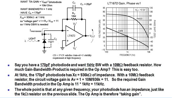
     I had read an article about transipedance amplifier (TIA) that explains how to figure out the TIA's GBW as shown below.

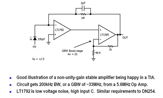
My first question is :does this explaination useful in an composite circuit ? Bescuse the article gives a circuit desgin "Speed up a JFET-INPUT OP AMP " as shown below. The GBW is 33MHz ,which does not equal to Gain(471)*Bandwidth(200KHz)=83.4MHz. The Gain 471 is from 1+1M / X330pF=1+1M / 2.4K=471. So I confused.


The next question is : In this composite circuit , what is the relationship between the Av of Boost stage and the whole circuit GBW? How can I choose other op amp to replace the LT1792 and LT1395? Can OPA 635 be the first op amp to replace LT1792 and op27 be the second op amp to replace LT1395?

Thanks!

Best Regerds!

Eva

  • Eva,

    I believe that the discrepancy in the calculations is due to a typographical error... 33 vs. 83.

    The OPA635 has a very large input bias current and is not well-suited to a 1M-ohm transimpedance application. I suggest that you explain your desired requirements including transimpedance gain and bandwidth. It may be possible to select an op amp that provides the necessary bandwidth without using the composite amplifier approach.

    Regards, Bruce.

  • Thanks Bruce,

    I made a mistake, it was OPA637 that I want to use, not 635. OPA 637 has a very low input bias current, and  very low noise.

    Actually I need a10^9 transimpedance gain with the desire bandwidth 4KHz(@-3dB), and very low noise. Ideally inverting feedback I-V circuit with a 1Gohm can meet the need. But  due to the parasitic capacitance across the large feedback resistor, the bandwidth is limited. Now  I obtain a citcuit which uses cascaded circuit, first stage uses a composite op amp to achive 5*10^8 gain, the second stage uses a simple invert feedback circuit which gain is 2.The first stage is similar to the composite op amp that I inserted in the first post, the difference is that there is a capacitance between the outputs pin6 and the pin2 of the first op amp.

    So I want to figure out the relationship between Av of the GBW boost stage and the whole composite op amp GBW. Then I will know if opa637 meets the GBW requirement .

    Thanks

    Best Regards!

    Eva

  • I missed a question, noticed that in the second picture I inserted in the post , the auther said LT1792 is low voltage noise,high input C. I mean in this transiimpedance circuit shouldn't we use a low input C op amp, for the input C of the op amp will be seen as a part of Cin of the source which will make the circuits unstable. 

  • Eva,

    Can you please provide a schematic of your circuit? A word description leaves too much chance for misinterpretation and error.

    You have not mentioned the capacitance of your photodiode or other source. This is important in determining gain-bandwidth requirements. Yes, the input capacitance of the op amp contributes to the gain-bandwidth demands on the op amp. Low voltage noise in the op amp is achieved by using very large input FETs... this makes high capacitance.

    For lowest noise, it is best to put all the gain in the transimpedance circuit. I understand that this may be difficult given the large transimpedance gain and desired bandwidth. Series connected feedback resistors may be able to reduce stray capacitance.

    Gain-bandwidth of the composite amp is equal to the gain-bandwidth of the first amp times the closed-loop gain of the second amp.

    Have you simulated your circuit with a SPICE program such as our TINA. This is a good way to test various possibilities.

    Regards, Bruce

  • Thanks Bruce,

    Thank u for your advice of TINA. It is very heplful ! 

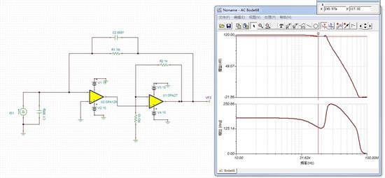
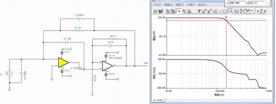
    I first simulated the composite op amp as a TINA learner . The circuit and the closed-loop gain is shown below


    Before simulate, I calculate the ideal f-3dB , assumed the GBW of the composite op amp  is 1M(opa129)*101(the second stage ). When I got f-3dB=231KHz,  I can get Cf .

    Then I take the  simulation, from the bode diagram we can see the -3dB f is ~245KHz.

     The simulation proves you are right !

    But another question is following:   the transfer function of this simulation circuit is practically the same as that of RC low-pass filter consisting of the feedback resistor and capacitance . 1Mohm with a 0.8pF will limit the frequency max 198KHz. But we get a 245KHz f-3dB, how can I understand this discrepancy?

  • Eva,

    The OPA27 has a GBW of 8MHz. In a gain of 101, this stage will only have a bandwidth of 80kHz. The pole that this creates inside the larger feedback loop is sure to create serious stability problems. The frequency response simulation will likewise be quite strange. You need a second op amp with much greater GBW.

    I changed the OPA27 to an idealized op amp model with GBW = 1GHz. This produced the expected rolloff of approximately 200kHz.

    You can experiment with the GBW of this second op amp using the idealized op amp model in TINA. This blog explains how to do it.

    Simulating Gain-Bandwidth—the generic op amp model

    Regards, Bruce.

  • Bruce,

    Thank u~  I  do appreciate your help!

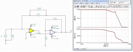
    I read your blog, then I changed the opa27 to an idealized op amp, yes ,it produced the exected rolloff of ~200kHz. But in a high frequency about 6MHz,it has a overshooting, should I care about it?

    And I add two capacitance in the circuit(just like the circuit I mentioned before) , it produced a larger bandwidth than the R(1M)C(0.8pF) limited frequency 198kHz .

    How did these two capacitances compenstae the bandwidth? Did they add some poles to the Aol of the composite op amp? Or they produced another feedback loop?

  • Eva,

    Several problems have made our previous simulations wrong:

    1. I made an error in simulating the 1GHz GBW second op amp
    2. Your model for the 1GHz op amp is also wrong.
    3. The macro model for the OPA129 is wrong. Its GBW is 15MHz and should be 1MHz.

    I have attached a TINA file with correct generic models for the OPA129 and the 1GHz second amp. The bandwidth simulations seem correct, now. The -3dB bandwidth is now approximately 310kHz. This is somewhat greater than the R1-C2 pole would predict due to some peaking in the response. The GBW of the composite amplifier is 100MHz. The noise gain of the circuit is 1+C1/C2= 376. So the bandwidth of the loop is 100MHz/376 = 266kHz. This limited bandwidth of the loop causes the peaking in the closed-loop response.

    Your second circuit will be grossly unstable. For stable operation, the single pole response of the OPA129 must dominate to, and somewhat beyond the bandwidth of the loop. Additional poles at frequencies less than this bandwidth will cause stability problems. This is control systems or feedback system theory--a good topic for study. Composite amplifiers can be very tricky and a thorough understanding of control system theory will help.

    Regards-- Bruce.

    6281.Composite TIA.TSC

  • Bruce,

    I need sometime to study and real understand what you said .

     You mentioned noise gain-----a concept I was not clear understanding of.

    1. Because in the handbook of operational amplifier application(SBOA092A), it used the rate of closure between the closed loop gain and open loop gain to see the stanbility of the circuit . But in SBOA055A , it said the noise gain determines the stability of the circuit. 

    2.  In the book 'op amp applications handbook' wrote by Walt Jung, the noise gain defination is the inverse of the net feedback attenuation from the amplifier output to the feedback input. And also has another concept ----signal gain.

    What's the difference between noise gain ,signal gain ,closed loop gain? I was lost .....

    And I was thinking back to the first post I wrote, the ways to figure out the GBW of the transimpedance amplifier circuit. When catulate the voltage gain of the circuit, why the Cf is not considered?  May Av=1+(1M//Xcf)/XcD  ?

    Thanks

    Best regards!

    Eva


  • Eva,

    Understanding of this subject will come in bits and pieces and you are consulting some good sources. You may want to read these blogs for further insight:

    Why Op Amps Oscillate—an intuitive look at two frequent causes

       Taming the Oscillating Op Amp

       Taming Oscillations—the capacitive load problem

    The Inverting Attenuator, G = -0.1… is it unstable?

    SPICEing Op Amp Stability  using SPICE to check stability of op amp circuits

    Regards, Bruce.

  • Hello All,

    For the circuit which Eva uploaded on April 7 (shown below), the bandwidth cannot be 200kHz (1M || 2pF results in 80kHz and not 200kHz), as stated.

    They must have possibly computed the 33MHz (noted within the image) based on:

    80kHz * 415= 33MHz (where 415 is the Noise gain for 330pF @ 200kHz!)

    However, the 415 is the Noise Gain (NG) assuming 200kHz (and not the corrected 80kHz). Here is the revised NG:

    NG (80kHz)_revised = ~ 1M * 2*pi()*80kHz* 330pF = 166 V/V

    GBW_revised= 80kHz * 166 = 13.3MHz

    So, you can get the 33MHz in the picture, if you compute the BW (80kHz) correctly but compute NG incorrectly (use 415 instead of the correct 166). My guesss is that a whole bunch of GBW has been thrown away here (5.6MHz * 21= 118MHz vs. 13.3MHz achieved) to compensate for the phase shift that the 2nd stage produces). So, it seems like there are some errors in this picture.

    Regards,

    Hooman

  • Hello All,

    I've simulated the composite amplifier circuit that Vera has uploaded using the device macromodels and confirmed an overdamped response of <90kHz. Note that if CF (2pF) is lowered, it is possible to get I-V bandwidth which exceeds 1/(2.pi()*RF.CF) due to underdamped response. This might have been the reason for the 33MHz GBW number (but possibly somebody forgot to note the reduction in CF on the schematic). CF = 1pF results in ~200kHz of BW with 5% overshoot (based on simulation alone).

    Regards,

    Hooman

  • Hi Hooman,

    I got a question about computing NG in this composite circuit.

    You had  NG (80kHz)_revised = ~ 1M * 2*pi()*80kHz* 330pF = 166 V/V.  Why don't we consider of Cf?

          may  NG=(1M // Zf) / Zcd where Zf is the impedance Cf @ BW ,Zcd is CD @ BW  ?

    Thanks

    Regards!

    Eva

  • Hi Eva,

    Sorry about the late response as I've been away from office.

    I think you can include the impedance of CF across RF when you are computing Noise Gain, for more accuracy. I agree with you.


    Regards,

    Hooman