Other Parts Discussed in Thread: THS3061, OPA847, THS4031
In the datasheet of the THS3061, the plot of “COMMON-MODE REJECTION RATIO vs FREQUENCY” shows CMRR gets worse with high frequency. Is this correct and if so, why does this happen?
This thread has been locked.
If you have a related question, please click the "Ask a related question" button in the top right corner. The newly created question will be automatically linked to this question.
CMRR depends on a number of design choices within the amplifier, but basically depends on the loop gain of the amplifier. With high loop gain, the error signal across the input terminals of the op amp is driven to zero and CMRR is high. At low frequency where the loop gain is high, the error signal is very low and CMRR is high. With low loop gain, the error signal across the input terminals of the op amp is high and CMRR is low. As frequency increases and loop gain decreases, the error signal across the input terminals of the op amp increases. The larger error signal across the input terminals of the op amp intern leads to lower CMRR. I hope this clarifies the behavior.
Hi ,
Thank you for the information.I ve got a couple of questions
The error signal that you are refering here is the common mode signal or offset voltages or both??
Also can you tell me how the offset voltages,the dc offset due to input bias current, will affect the CMRR?
Stephen,
A 'regular' differential input to single-ended output op amp has a non-zero common-mode gain due to its architecture (since it is single-ended output) which results in a non-infinite CMRR (= differential gain/common mode gain). Instead of thinking in terms of a physical error signal across the + and - inputs, you might think of it this way instead: with the two op amp inputs shorted together at a voltage Vcm, the ideal output should be 0V since there is no differential signal, however, due to non-infinite CMRR, there will be an output offset voltage. This output voltage offset can be referred to the input as an input offset voltage but this is a separate offset than input offset voltage and offset due to bias currents.
Input offset voltage and input offset current (resulting in a separate input offset voltage) are due to mismatch in the input differential pair (for a voltage feedback op amp). These errors are independent of the op amp's ideal CMRR (assuming perfectly matched inputs). In practice, however, the measured CMRR of the op amp and the CMRR of your application circuit will depend on many different sources of error working together - op amp offsets, op amp CMRR, resistor tolerances, etc...
Hi,
Thank you for the information. I understand that the effects caused by the external components do affect the CMRR of the circuit in a separate way other than the CMRR of the opamp itself.
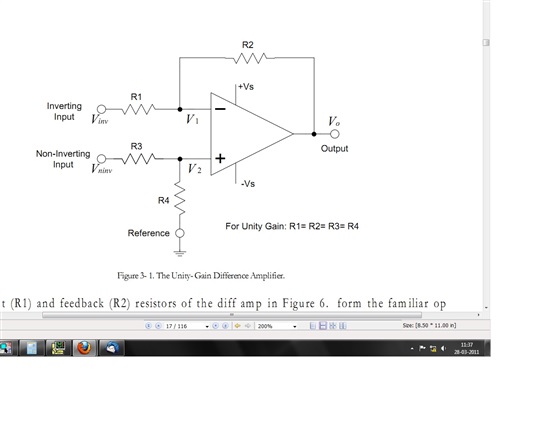
I was looking to the unity gain Differential amplifier circuit built using an op-amp.Since it is unity gain all the resistors are the same.
But it can be 10k or 100k or any other value.But How it will affect the CMRR? or what other parameters are affected by the values of these resistors?Or precisely how is it to be selected?

Thanks & Regards
Stephen
Stephen,
If the resistors are perfectly matched, then the low frequency CMRR should not be affected by the value of the resistors.
Larger resistor values will increase the output noise of the amplifier (see Noise Analysis for High Speed Op Amps - sboa066).
The + and - input pins of an op amp will have some parasitic capacitance which will form RC low pass filters with the resistors that can limit the bandwidth of your circuit. The approximate input pin capacitance values are included in most TI op amp datasheets.
Also, for high speed amplifiers, the feedback pole formed by the feedback resistors and the inverting pin capacitance can affect stability since the pole results in more phase shift in the feedback. The higher the resistor values, the lower the pole frequency and the more phase shift at lower frequencies. Our high speed op amp datasheets list the feedback resistor values used to generate the Typical Characteristic graphs. For current feedback amplifiers, where the feedback resistor value determines the op amp's compensation, we usually include a table of recommended feedback resistor values for various gains. It is a good idea to use resistor values close to those listed in the datasheet.
As you mentioned, the input bias currents will result in an offset voltage, since the bias currents will develop voltages as they flow through the equivalent resistances looking out of the + and - input pins. Therefore, larger resistor values can lead to larger offset voltages. See p. 26 of the THS4031 datasheet and p.17 of the OPA847 for some discussion on offset due to input bias currents.
The above was purely qualitative, but hopefully it is helpful. You should be able to see some of the above effects through simulation with our op amp models in TINA-TI and varying the resistor values.
Thank you Kristofer,
So as the resistor values are increased
1)Bandwidth is decreased
2)Noise voltage is increased.
Hence i suppose the offset errors tend to increase..& hence CMRR should decrease.
I tried the simulation method used a Pspice model and tried to plot some curves..i tried to vary resistors 10k to 100K and got the resultant CMRR varied though in and around 5dB.
So i think the resistors values doesnt have that much grave effects on CMRR.Im attaching my simulation results ...I got some random variations..& CMRR high towards 100k than obtained at 10k.( but its not perfectly correlated since 10k got better CMRR than 20k & 30K ,,though that confused me).
Im attaching my simulation results .. that you may take a look
Thanks .