Other Parts Discussed in Thread: OPA357, TLV3501
Hi all,
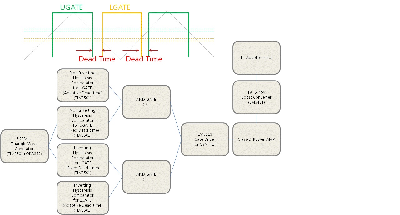
I am developing Class-D Power AMP(35W, 6.78MHz) for wireless charge.
The plan to make a circuit is as below picture.
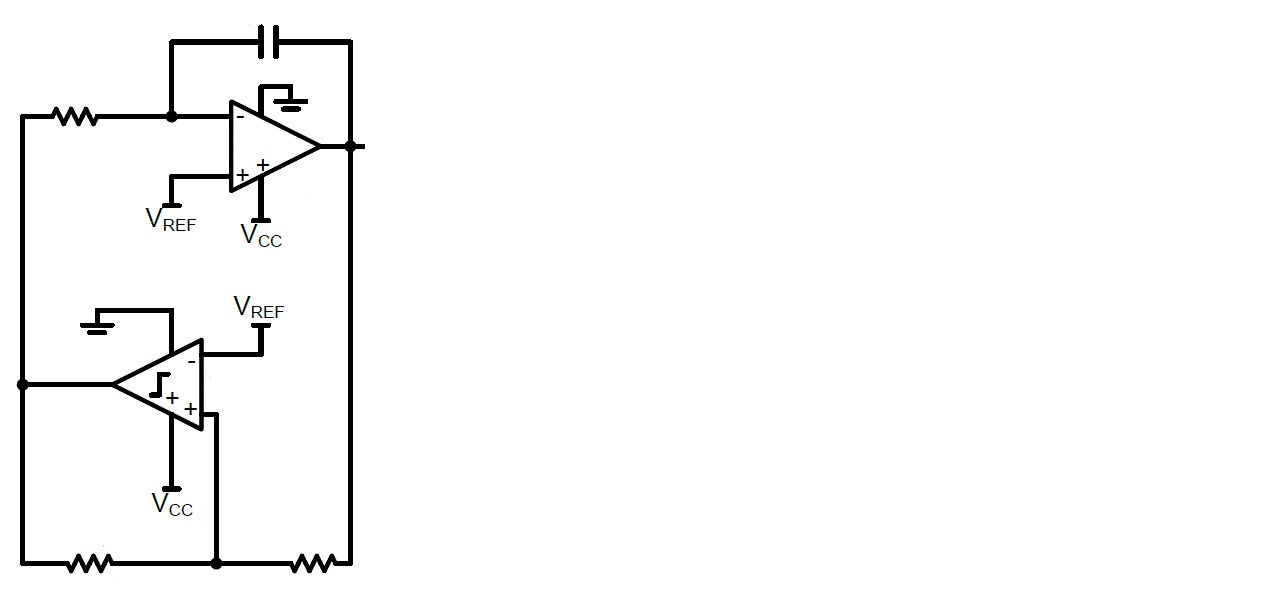
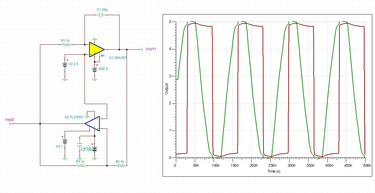
Triangle wave is made by TLV3501+OPA357 and then it make pulse which will drive FET gate and have a dead time by using comparator.The specification of Op-Amp for 6.78MHz should be more than 40~60V/us for slew rate and 130MHz for Bandwidth.
I would like to know that this process is right for signal to Gate driver.
Could you give me some advice for this plan? please recommend proper device if some device is wrong.
Thank you for your help.