This thread has been locked.

If you have a related question, please click the "Ask a related question" button in the top right corner. The newly created question will be automatically linked to this question.

Load cell amplifier (INA111 + OPA)

Other Parts Discussed in Thread: INA111, OPA211, ADS7883, OPA227, OPA37, INA331, OPA333, LMH6647, OPA365

Hi,

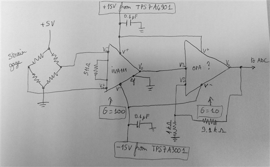
I want to amplify the signal from a load cell for dynamic applications, and I need a overall gain of 1000. The problem is that the signal frequency I'm interested in may go up to 1 MHz. I figured that I should use a INA111 with a gain of 100, which should work fine at 1 MHz, followed by an op-amp in closed loop set up with a gain of 10 (see picture). 

Hence the following questions:

1. Does this make sense? Or is it better to use the INA111 with a gain of 1000 alone, but in this case I won't get the high frequency in my signal, right?

2. Which OPA do you recommend for this application? I would like to use the same power supply as the INA111, so +-15V ideally.

3. I want to prototype this on a breadboard, and I'm concerned it might oscillate. Do you have any tip to make sure it doesn't happen?

Note: I am a mechanical engineer, I wouldn't say that I have no idea what I'm doing, but I am definitely not a specialist.

Many thanks!

Baptiste

  • Hello Baptiste,

    A load cell with a 1MHz bandwidth seems extremely high to me. Are you certain this is the case? What is the part number?

    Also, what is the input voltage range of the ADC?

    Note that the bandwidth of the INA111 at G=100V/V is 450kHz, so you should reduce the INA gain to ~10V/V. Unfortunately that means you require a high bandwidth op amp for the gain stage. The OPA211 provides excellent offset considering it has a bandwidth of 80MHz, however I don't think that will be enough for your application.

  • Hi Peter, thanks for your reply.

    Yes maybe 1MHz is an upper value, in reality the signal frequency should be closer to 50-100KHz which should be alright. 1 MHz will be the sampling frequency. 

    The ADC is the ADS7883 (input range 2.7-5.5V). 

    Is there a OPA similar to the OPA211 but with DIP package?

    Thanks

  • Hello Baptiste,

    Thanks for the additional information.  50-100kHz still seems significantly high to me.

    Nonetheless, the OPA227/8 and OPA37 have high BW, low offset voltage, and come in DIP packages.  Please note that there are "DIP adapter boards" that you can use to convert surface mount packages to DIP packages.  They are available at a number of online electronics retailers.

    Given that your bridge voltage is 5V and the ADC is 5V, I caution the use of +/-15V supplies for
    your analog signal conditioning.  The output voltage of the INA and op amp depend on the supply voltages.  If, for some reason, the input to the op amp (assume OPA211) experiences an anomoly, the output could saturate near the supply rails (e.g. +/-14.8V).  This would not be good for your 5V ADC.

    Therefore I recommend either reducing your analog signal conditioning circuitry supply voltage to 5V or using diodes to protect the input of your ADC.  If you reduce your supply, though, beware of the corresponding reduction in output swing of the INA111.  You may then want to consider the INA331 for its output swing, but at the expense of offset voltage. 

  • Hi Pete,

    Thank you very much for your help. 

    Indeed it makes sense to use 5V for the load cell, ADC, INA and OPA. In this case, does this still make sense to use a negative linear regulator? It doesn't seem necessary, the no-load value would not be 0V but that can easily be compensated in the software. 

    So I could use one 5V linear regulator to provide power to the whole chain (150mA should be enough for all the components, right?). 

    The chain would then be

    Bridge (input: +5V, ground, output: 0 to 3mV)-----INA331 (input: 0 to 3mV, power: +5V, ground, output: 0 to 300mV)-----OPA227(input: 0 to 300mV, power: +5V, ground, output: 0 to 3V)-------ADC(input: 0 to 3V, power: +5V, ground)

    Would that be OK? Do you think I can prototype this on a breadboard without being concerned about it oscillating? The only thing I have in mind is to put a 0.1 uF capacitor after the linear regulator.

    Thanks again!

    Baptiste

  • Hello Baptiste,

    Unless there is some other component that requires a negative voltage supply, I see no need for it in this solution. Yes, you could use a single 5V supply for the entire system.

    Concerning you signal chain description, please understand that your bridge sets the common-mode signal of your input. I assume that when you state your input is 0-3mV, you're talking about the differential voltage. It is important to ensure that your input common-mode voltage is in the range of the INA (usually mid-supply), so be sure to set the other resistors in the bridge appropriately.

    One additional recommendation: drive the reference pin of the INA (assuming you use the INA331) with 100mV (simply divide down the 5V supply and buffer with an OPA333). Then, when the differential voltage of the bridge is 0, the output of the INA will be 100mV (ideally). Any discrepancy is most likely due to resistor tolerance and the offset voltage of the INA. Therefore you will likely calibrate out the errors by comparing the ideal output with the actual unloaded output.

    Personally I recommend building a PCB instead of prototying it with a breadboard. I think it will still work using a breadboard (and probably won't oscillate), but the use of a PCB removes a number of variables when prototyping. For example, breadboards have resistance and capacitance associated with their connectors. In addition, the expansive use of wires and leaded passives for this large of a project invites shorts, bad connections, and potential interference.

  • Hello Pete,

    Thank you for your advice. I will build a PCB but I need to be sure that my wiring is correct. Can you check the attached pdf to see if I got it right?

    0407.DAQ_schem.pdf

    Base on this wiring, I have two questions:

    1. I am only interested in one loading direction, that's why I wrote that the differential output of the bridge is +3.5 mV. This translates to a final signal from 1 to 4.5 V. But what if the load cell is loaded the other way? My understanding is that I will have a differential output of -3.5mV, so the INA will output from -250mV (impossible) to 100mV, so in reality it will hit the ground rail and output zero when the input is negative. Is that correct? Is that a problem (knowing that I don't care about the signal in this direction, but can it damage the next components?) ?

    2. In the documentation of the OPA227, it says that the source impedance has a direct influence on the output noise. I have the INA111 just before, what is its impedance? Should I be concerned by that?

    Thanks again for you help

    Baptiste

  • Hello Baptiste,

    Here are some suggestions:

    1) I think this was drawn in MS Paint. I recommend using the schematic capture program from your PCB tool of choice for schematics (e.g. PCB Artist). That way you don't have to draw it multiple times.
    2) I assume that this is all single supply, so just use a GND symbol for the GND net. That makes it much easier to read.
    3) There are no power supply decoupling caps shown for the INA or op amps
    4) I suggest using precision resistors (0.1%) for just about everything, especially your voltage divider and bridge resistors. I see no need for anything of worse tolerance than 1%.
    5) When drawing a diagram, use the actual device symbol...not the package. It is difficult to quickly understand the signal path when drawn with packages instead of the traditional op amp and INA symbols.

    If the load cell outputs a negative differential voltage then the INA's output will try to get as close to the negative supply (GND) as possible.  For the INA331 that will be ~25mV (see INA331 output swing specification in data sheet).  This will not damage the device or other devices further down in the signal chain.

    For your second question, I assume you mean the INA331, not INA111.  The output of the INA331 is the close-loop output impedance of an op amp (A3), which is going to be very small.  So, you will be just fine.

  • Hello Pete,

    I used Fritzing to draw this schematic, it is able to generate PCB images. Unfortunately I can't use the device symbol in this software.

    I added decoupling capacitors before the INA and the 2 OPAs, and also changed some of the resistors for trimpots so that I will be able to adjust the gains from the INA and OPA227 and the offset from the OPA333 later. Do you know if that's a problem? I don't think trimpot values drift over short periods of time. 

    I also will use precision resistors as suggested.

    Here is the updated schematic: 1423.DAQ_schem.pdf

    I will try to have this PCB made at the university, I will let you know if it works as it should!

    Thanks again for you help.

    Baptiste

  • One more thing:

    I tried to check the schematic using the TINA software. Everything works fine except the second amplifier (OPA227). It seems that this op amp is not suited for single-supply operation. 

    Could you give me an alternative product that I can use with my +5V power supply and the ground as ref? This last stage consisted in amplifying a signal ranging between +100mV and +450mV to a signal ranging from +1V to 4.5V.

    I tried with another op amp, the LMH6647. It works as expected with my single power supply, but it is not a precision amplifier.

    Many thanks!

    Baptiste

  • Hello Baptiste,

    I recommend evaluating the OPA365.