Other Parts Discussed in Thread: OPA564
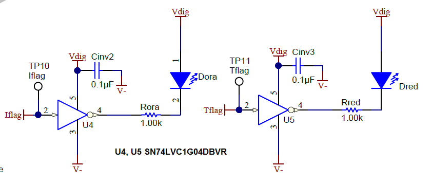
Are the the digital flag outputs, push pull outputs? The datasheet seems to apply that they are. I was testing my design in TINA and I am not seeing the current flag increase rise when the output is clamped/limited.