This thread has been locked.

If you have a related question, please click the "Ask a related question" button in the top right corner. The newly created question will be automatically linked to this question.

TL07xx Low-Noise JFET-Input Operational Amplifiers

Request you to please confirm

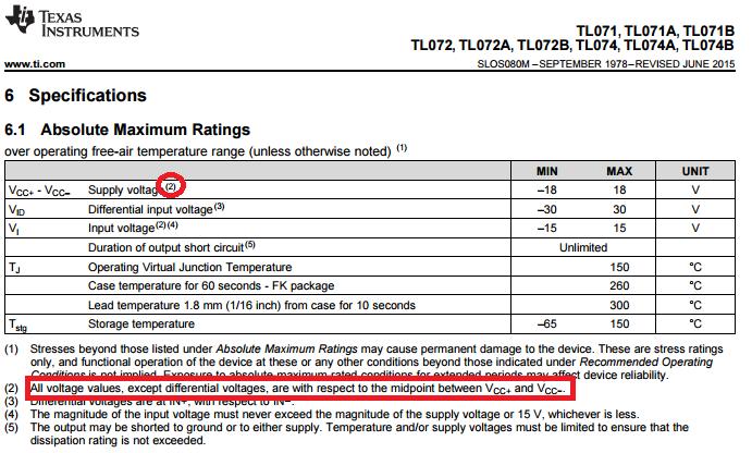
Vccpos – Vccneg rating mentioned in the Maximum rating section of new datasheet has range of -18v to 18v

but the old datasheet mentions VCC+ to be 18v max and VCC- to be -18v min

what is the maximum & minimum value VCC_positive supply can take ?

what is the maximum & minimum value VCC_negative supply can take ?

 regards

Siddharth

  • Siddharth,

    There is no internal ground pin inside the op amps, including TL07xx, thus the power supply voltages can be anything you want as long as the total power supply voltage between positive (V+) and negative supply (V-) does NOT exceed 36V.  Therefore, they could be +18V & -18V, 0V & 36V, -36V & 0V, or 100V & 136V, etc.  Of course, if you shift the power supplies you have to make sure that the input and output voltages stay within your supplies - see link below for more information.

    https://training.ti.com/ti-precision-labs-op-amps-input-and-output-limitations?cu=14685

  • thanks do you mean VCC_POSITIVE - VCC_NEGATIVE should at maximum be 36v ? So then why is the figure 18v indicated under the Max column? Also what is the minimum value that the expression VCC_POSITIVE - VCC_NEGATIVE can take? regards
  • Siddharth,

    Yes, the total supply voltage is VCC_POSITIVE - VCC_NEGATIVE or  (V+)-(V-) in case of TL07xx must be less than 36V.

    Please read the note (2) above:  All voltages are with respect to the midpoint between Vcc+ and Vcc-.  Thus max +18V is with respect to the midpoint whatever it might be; if supplies happen to be 100V & 136V, the midpoint is 118V and thus MAX supply can be 18V above it (118V+18=136) and MIN supply 18 V below it (118V-18V=100V).

    The Absolute Minimum value for the total supply voltage is 0V (you should never reverse supplies-this prevents damaging the part) but specified minimum value for TL07xx total supply voltage (for the circuit to work properly) is +/-9V - see below:

    I think you should review material discussing op amps under link below:

    http://www.ti.com/lsds/ti/amplifiers-linear/precision-amplifier-precision-labs.page

  • ok thanks i will do that. A Functional block diagram is given on page 13, can i have the resistor, capacitor etc.. components values only few of them are mentioned, also if you have a spice model which might run on LTSPice or something please do let me know. regards
  • The only reason for showing TL070xx functional diagram in our datasheet is to inform you how it is protected against ESD/EOS and what may be required to implement additional external protection depending on customer’s specific application.  This is a functional schematic and NOT an actual circuit that may be significantly different from what is shown in order to protect TI intellectual propriety   For that reason, I cannot provide you with component values beyond what is already shown below. 

  • thanks for the reply, you mentioned about device protection-
    1. Can you please confirm which components are doing that job
    2. is there any way to reduce the current consumption of this JFET input functional block diagram?
  • Hi , ANY FEEDBACK over -last post 

    REGARDS

  • SIDDHARTH,

    1) No ESD cells are shown in schematic. The schematic is not exact but very close.
    2) Try TL03X and TL06X op amps for lower ICC.