


Other Parts Discussed in Thread: OPA454
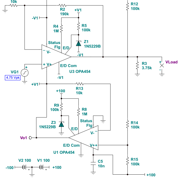
[ OPA454 ] E/D and E/D Com Connection
Hi expert,
Can you help me to understand the detail of E/D and E/D Com pin more clearly?
As I indicated below, we have some options to disable “ENABLE/DISABLE” function (let OPA454 output always on).
However, the last approach “Choosing RP to be 1 MΩ with a +50-V positive power supply voltage results in IP = 50 μA.” is confused me a bit.
I’m not sure whether this approach does meet with absolute max specification of E/D and E/D Com pin.

Also, datasheet suggests the different approach to keep output stage on.
It’s really appreciated, if you can help me to understand!
Thanks,
Ken
Other good references
OPA454
e2e.ti.com/.../226867
OPA454 E/D logic connection
e2e.ti.com/.../268763
OPA454 shutdown operation
e2e.ti.com/.../518375
OPA454 - Cannot enable output; E/D draws large current
e2e.ti.com/.../1501684


