This thread has been locked.

If you have a related question, please click the "Ask a related question" button in the top right corner. The newly created question will be automatically linked to this question.

LM6132: Low Temperature current limit.

Part Number: LM6132
Other Parts Discussed in Thread: LM6142,

Hi There,

I have a circuit that uses an LM6132BIM to drive a sine wave into multiple loads.

Op amp supply voltage is +/- 14V

Sine wave is ~ 5VAC , around 7.5V Peak.

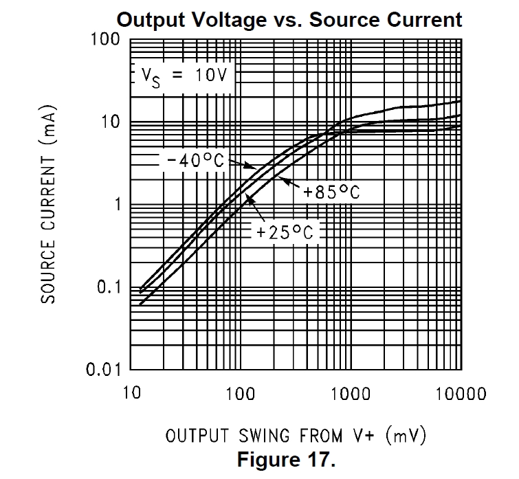
At -40 Deg the sine wave has noise at the peak.  The data sheet has a figure:

That shows a current limit, but I'm not sure what "Output Swing from V+" means.  Is there a relatively straightforward answer for the current limit under these conditions?

This is a circuit and a test that we have used for 10 years, and we have recently had 2 very similar failures.

I've not attempted to simulate the circuit yet.

Thank you,

Jim

  • Hi Jim,
    Do you have a scope photo of what you're observing to attach here?
    The figure in the datasheet you referenced did not come through! Can you please try to attach gain or specify the Figure number?

    Regards,
    Hooman
  • Thanks for looking at this. 

    I'm referring to figure 21 of the datasheet.

    NCMR 3508 5VAC Investigation.docx

    Scope trace of my issue:

    Normally the Channel B & D Traces (Red and Yellow) are smooth at the peak.

    Channel A (Blue Trace) is the output of the 1st stage of a filter, Channel B is the output of the 2nd stage.

    Channel D goes through one more driver and then out to the sensor.

    Not sure my figures are showing up when I "Paste from Word", but it looks like I could attach a word document.

    Simulation shows P-P current requirements at the op-amp output about 8.85 mA.

  • Hi Jim,

    Thanks for the additional detail you provided.

    The "Output Swing from V+" x-axis in Figure 21 means the voltage at the output relative to V+ rail. If your circuit output swings to 8V and V+ = 14V, then the x-axis is 6,000mV. From that same figure, you are looking at typical output sourcing current of ~3mA (-40 deg. C). So, the fact that you could draw up to 4mA (= 8V/ 10k * 5_stages) says that you could be running into an output current limitation (as you've already pointed out). It is good to have some margin above Typical to account for device variations.

    As an experiment, could you install the LM6142 instead in that same socket to see if the problem can be resolved? The typical output current should increase to ~ 6 to 7 mA per Figure 17 shown below:

    LM6142:

    You would not have any issue with output sink current capability (LM6142 Figure 21) as it is > 15mA.

    The LM6142 consumes a little more supply current. These devices (LM6132 and LM6142) are otherwise compatible in every way with LM6142 having improved performance.

    Alternatively, you could try increasing the value of the following stage(s) input series resistor (R133, etc.) to 100k (from 10k now, 5 places - just like your Word attachment, item 4b states) to see if the reduced loading alleviates the problem? To keep the low pass roll-off characteristics unchanged, you could reduce the cap C14 to 100nF instead of 1uF currently.

    Please let me know so that we can resolve this issue.

    Regards,

    Hooman

  • Thanks Hooman, all good suggestions.

    Like I said, most of the time the LM6132 works under these conditions. In fact, when there is a failure, the unit heats itself up enough in 2 or 3 minutes (keeping ambient air at -40 deg) that the problem go away.

    I would consider this issue closed from this conversation.

    One piece I'm still confused by is the Absolute Maximum Rating for "Current at Output Pin = 25 mA" in table 6.1. How does that relate to Figure 19, 20, and 21?
  • Hi Jim,
    There is no direct relationship between the output current Absolute Maximum Rating and the figures you quoted.

    The +/-25mA limit must correspond to the current handling capability that could violate something within the die. Most likely, the output transistor size is the determining factor here having a certain collector current limit. The output current plots you quoted are all within / lower than +/-25mA and that is what you want them to show.

    If in fact you are being limited by output current, you are most likely to run out of base current drive for the transistor beta that your "problem" devices have. It is reasonable that there is a distribution of devices that fail while most devices have enough drive.

    Please let me know if you find out more about the cause of the issue after you run some experiments, as discussed earlier.

    Regards,
    Hooman