This thread has been locked.

If you have a related question, please click the "Ask a related question" button in the top right corner. The newly created question will be automatically linked to this question.

LM2902: Propagation delay between input and output

Part Number: LM2902
Other Parts Discussed in Thread: LM324

Hi all

Would you mind if we ask LM2902?

On our customer's circuit, there is big propagation delay between input and output.
We think it is cause of customer's circuit.
So, at the first we would like to share the circuit.

However these files inculde confidential content.
Could let us know your E-mail address?(We would like to send you the file.)


Kind regards,

Hirotaka Matsumoto

  • Hirotaka-san,

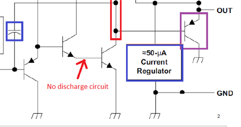
    Here is LM2902 (LM324) Tech-Day presentation that should explain the cause and solution.

    3173.TS321,LM358,LM324_Tech_day.pdf

  • Hirotaka-san,

    With a precondition of output at zero (load only to GND, not VCC) the red node (see pdf) will be near zero and the NPN source driver will be off. The red node will need to internally slew about 2.1V before NPN source driver can make output rise. This is about 2.0V/(0.5V/us) = 4us. There is also something call "overload recovery" time. This is the time between output at VOL or VOH level (open loop mode) getting back into a linear operation mode (closed loop mode). This accounts for the rest of the 7.2us delay seen.

    With a precondition of output at 0.4V (load only to GND, not VCC) the red node (see pdf) will be near 2.4V and the NPN source driver will be on. Any rise on the red node after the input pulse will immediately be reflected in a rise of output voltage. Because the output is not at VOL or VOH (open loop), overload recovery time is not applied.

    I studied the application schematic and wasn't able to find a way to keep the output in the active range with the NPN source driver alway on.
    I will give this more thought.
  • Ron san

    Thank you so much for your support and your advice.

    We would like to confirm one point.

    "This is about 2.0V/(0.5V/us) = 4us. There is also something call "overload recovery" time.
    This is the time between output at VOL or VOH level (open loop mode) getting back into a linear operation mode (closed loop mode).
    This accounts for the rest of the 7.2us delay seen."
    ->There is a bit idifference between 4us and 7.2us. We got that "This is about 2.0V/(0.5V/us) = 4us. There is also something call "overload recovery" time.
       The difference 3.2us, what is the cause? If you have some advice, could you let us know?

    Kind regards,

    Hirotaka Matsumoto

  • Hirotaka-san

    This is the most likely cause for overload recovery  (aka storage time)

    This node can go high quickly, turn off is much slower. 

  • Hirotaka-san,

    One possible solution is to add a resistor from 5V to pin 5 of LM2902 to get a VIL greater than 10mV (worst case VIO of LM2902)
    This will keep output active so it can respond quickly.
  • Ron san

    Thank you very much for your reply!

    OK, we got it!
    We would like to confirm one point.
    "from 5V to pin 5"
    ->It seems that 5 pin is 2IN+ or NC.Does it mean NC?

    Kind regards,

    Hirotaka Matsumoto

  • Ron san

    We are sorry to rush you, however could you give us the reply for our last update?

    "from 5V to pin 5"
    ->It seems that 5 pin is 2IN+ or NC.Does it mean NC?

    Kind regards,

    Hirotaka Matsumoto

  • Hirotaka-san,

    2IN+ is the pin.

    If noninverting input is alway a little positive then the output will be souring a tiny current and output will respond quickly.

  • Ron san

    Thank you very much for your reply!
    Ok, we got it.

    Kind regards,

    Hirotaka Matsumoto