Because of the holidays, TI E2E™ design support forum responses will be delayed from Dec. 25 through Jan. 2. Thank you for your patience.

This thread has been locked.

If you have a related question, please click the "Ask a related question" button in the top right corner. The newly created question will be automatically linked to this question.

THS4551: Sudo Differential input attenuation to differential output

Part Number: THS4551
Other Parts Discussed in Thread: ADS127L01, TINA-TI

Hello,

I have a rather unique problem. I am going to use a THS4551 as a differential adc driver for a ADS127L01. My issue is the stage before the THS4551 is a trans-impedance amplifier that will have a 0V to 10V output. The output will also be offset by a known DC voltage. So in this scenario, I will use the voltage offset as the sudo differential negative input and the TIA output as the positive input and both need to be attenuated by 1/4 so the TIA output can map to the ADC range.

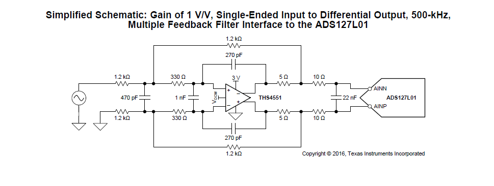
You have a reference design for driving the ADS127L01 in your datasheet,see below. I would like to know how to modify it to get the 1/4 attenuation on both the negative and positive inputs but not change the frequency response. I assume a simple voltage divider will work but I am new to FDA and Im not sure how to calculate the input impedance to get the attenuation right. Plus an resistance I add to the source will change the filtering properties.

Thanks,

John


  • Hi John,

    The only modification that needs to happen for the above MFB filter interface is replace the input 1.2kohms with 4.8kohms. Rest of the filter components could stay the same. I have attached a TINA-TI circuit simulation which shows a flat band response across frequency with ~300kHz cut-off if you want to look over.

    Best Regards,

    Rohit

    THS4551_MFB.TSC

  • Rohit,

    Thanks for the response. This all looks good by I will be running at 3.3V not 5V also a vocm of 1.65V since that is what the ADC called for. For some reason there is a odd clipping that occurs when I change these voltages . I see not voltages approaching the rails either on the inputs or outputs. can you explain and or fix this?

    Thanks,
    John
  • Hello TI,

    Would it be possible to provide the design equations for above circuit, or a spreadsheet incorporating these?

    I am also looking to modify this circuit, but for a cut-off of 43kHz and Gain options of 1 and 2 (using the ADS127L01's Low Latency filter, 128kSps and OSR=128).

    sloa054e does not include a derivative which includes the 5Ω output resistor.

  • John,

    If you are planning to run at 3.3V and not 5V supply, then you will be violating the THS4551 input common-mode voltage spec for the current circuit with 0 to 10V input voltage swing. Looking at the ADS127L01 datasheet, it has Vref nominally set to 2.5V which will require a 1.25V Vocm out of the THS4551. 

    I have attached the modified circuit below that takes care of the output clipping on a +3.3V supply. The THS4551 Vocm can be set to 1.25V on a single +3.3V supply because it has rail-to-rail output.

    Best Regards,

    Rohit

    THS4551_MFB_3.3V.TSC

  • Rohit,

    Thanks this looks good. The ADS127L01 datasheet says the common mode input voltage should be VCM = (VAINP + VAINN) / 2. With a 3.3V supply doesnt that mean my Vocm should be 1.65?

    Thanks,
    John
  • John,

    I think you are right that a 3.3V supply on the ADS127L01 will require a Vocm of 1.65V. If that's the case, then you will start seeing the THS4551 outputs to clip with 3.3V supply due to the limited input voltage headroom towards the positive supply while level shifting a 0 to 10V input. I think the only way to resolve this is by operating the THS4551 on +3.6V or higher supply voltage, while keeping its Vocm centered around 1.65V.

    Best Regards,
    Rohit
  • Rohit,

    Thanks for all your help on this. I think I'm am fine with this design but can you point me to a good white paper on doing a simple nodal/stability analysis on a FDA. For example, I have no Idea how you can up with the modifications to the attenuation and I would like to be able to explain them.

    Thanks,

    John

  • Hi John,

    You could look at the below link for understanding the stability of an FDA.

    training.ti.com/ti-precision-labs-–-op-amps-fully-differential-amplifiers-–-fda-stability-and-simulating-phase

    Best Regards,
    Rohit
  • Hi Bernhard,

    The MFB filter designed above is very similar to the details mentioned in the sloa054e document with a slight modification as you have noted that includes the 5-ohm output resistor. As such the design equations stay the same as the sloa054e document.

    You should be able to use the Webench Filter Designer for your application to design a single-ended filter and then port it over to the FDA for the differential filter topology. It is important to note that the parallel or shunt capacitors will become half in value for the differential filter topology. The link to the Webench Filter Designer is provided here: www.ti.com/.../webench-filters.html

    Let me know if you are having difficulties designing the 43kHz cut-off MFB filter.

    Best Regards,
    Rohit