This thread has been locked.

If you have a related question, please click the "Ask a related question" button in the top right corner. The newly created question will be automatically linked to this question.

TINA/Spice/OPA197: Difficulty with convergence issue in modeling + in stability analysis

Part Number: OPA197
Other Parts Discussed in Thread: TINA-TI, , OPA4197

Tool/software: TINA-TI or Spice Models

Hello,

I'm in the process of trying to model a unity gain follower using the OPA197 with various load capacitances but am running into some issues with TINA. Note that I'm a hobbyist, not an EE, so I apologize in advance for any dumb questions!

First of all - in the attached file "opa197 unity gain", which is just the simple unity gain follower circuit, I am getting the error "Convergence problem. Check the analysis parameters".  I'm not sure exactly why its having difficulty with the circuit as it seems pretty basic...

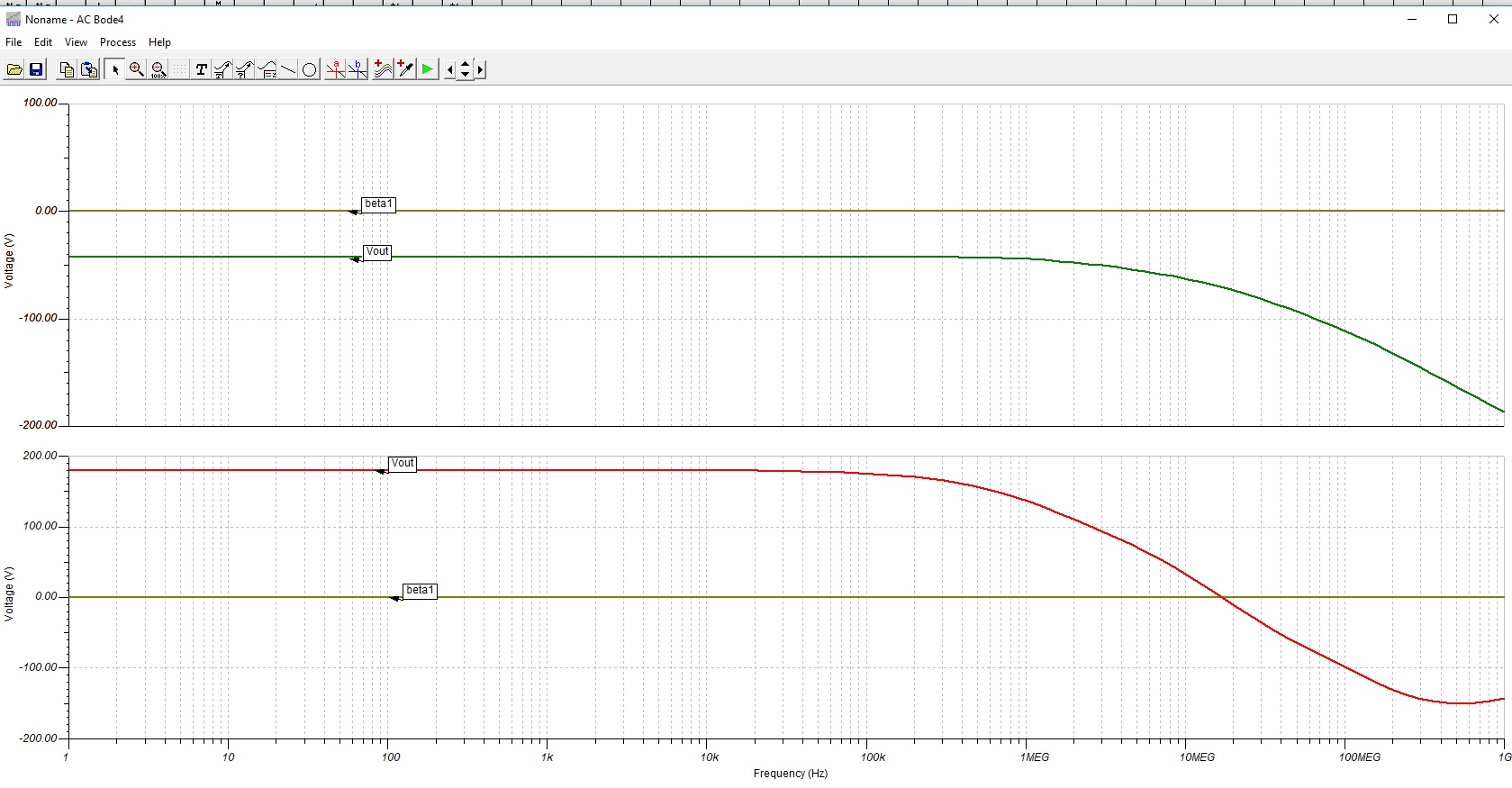
Secondly, in the attached file "opa197 unity gain stability analysis", I've attempted to follow the instructions in this tutorial in order to get look at the phase margin for the circuit (). However, The curves that are being generated look very strange, and the baseline open loop gain seems to start from -50db... I'm not certain as to why the curves are coming out wrong (see attached image). Can anyone give me a hand?

Thanks so much in advance..

  • Victor,

    Please see the attached circuit opa197 unity gain stability analysis_revd.TSC.
    It is the same as your circuit except the power supply has been changed from a single +12V supply to two supplies with voltages of to +6V and -6V.
    The resulting open-loop gain & phase - shown in the right-most top plots - are much closer to  those shown in the schematic's original graphics.
    The reason this helped is because the pins of the original circuit are at about 0V, which forces the simulator to bias the circuit for an operating point at ground which won't allow a meaningful signal swing.

    By changing the power supplies to -6V and +6V, the 0V bias point is at the mid-point of the power supplies.
    This is an optimum bias point from the standpoint and it allows the greatest amount of signal swing.

    The other circuit seems to have an issue with the 500pF  load capacitance.
    If the load capacitance is reduced to 1pF, the AC response changes to the expected behavior.
    The device data sheet makes some recommendations in Table 3 for values of Riso for given values of Cload. 
    Based on the table, I'm guessing the resistor between the amplifier and the load resistor needs to be larger.

    If none of this helps, I can move this thread to the E2E Amplifiers forum that is monitored by the product experts.
    Please let me know if that is what you want me to do.

    Regards,
    John

    opa197 unity gain stability analysis_revd.TSC

    opa197 unity gain_revd.TSC

  • Okay - thanks that's very helpful. The datasheet however does indicate that the opamp should be stable directly driving loads up to 1nf... The convergence issue seems resolved with the switch in supply voltage that you did, and the DC offset I was seeing in the ~235mV range is also solved. However, in the circuit I'm designing, its a retrofit as an output buffer for a gamma signal in a TV... and as far as I can tell there are no -ve supply lines around (the schematics for the board are not publicly available - I'm having to reverse engineer...), however there are both +12V and +24V supply voltages, so I was going to use the 12V voltage. Is this going to be an issue like in the simulation, or is this simply a simulator issue?

    Thanks so much,
    Vic
  • Victor,

    At this point it would be best to weigh in with the product experts that monitor the E2E Precision Amplifier Forum.
    I will move the thread to that forum and they can help with questions on the actual device.

    Regards,
    John

  • Sounds good - thanks very much John for your help.
  • I am glad to help Victor.
    Please let me know if you have any more questions.
    John
  • Hello Victor,

    Thank you for your patience during the holidays. The OPA197 can operate just fine on a single +12V supply, however it's advised in this case to bias the input signals up to mid-supply (+6V) to make sure the amplifier operates in the linear region. If not you can see large offsets and incorrect transfer functions appearing when you try to verify the circuit behavior in simulation.

    I've modified both of your original circuits to work better at single-supply by biasing the input signal to +6V. You can easily do this with a resistor divider if you have access to the +12V node on your board. The stability test with Riso = 10 and CL = 500pF had over 60 degrees of phase margin, so there should be no stability issues in that configuration.

    opa197 unity gain_ss.TSC

    opa197 unity gain stability analysis_ss.TSC

    Best regards,

    Ian Williams
    Applications Engineer/SPICE Model Developer
    Precision Amplifiers

  • Hi Ian - very sorry for my own delay in responding. Thanks for the help here - part of the problem, is that the application is actually using 9 parallel channels for 9 DC reference voltages that provide reference gamma voltages for an OLED panel, all with different voltages. In the interim, I've actually built the circuit and its working without issue so far (just finished it today). The 500pF value in the tina spice model I supplied is actually a complete estimate of the load from the traces, ribbon cable, and unseen circuit along the panel itself I can't access. Unfortunately, I don't have schematics, so I'm reverse engineering... The circuit hasn't completely solved the issue I'm having with the TV - I'm trying to fix a widespread banding issue in the LG OLED TVs, which I currently believe is due to oscillation from the gamma chip they're using - which I thought was likely due to the capacitative loading on the chip (single chip runs 9 channels, and there are snubber circuits on the output of each to isolate it). ..

    Anyways, I'm likely going to try implementing the precision reference buffer schematic found in the datasheet for the OPA197 next..

    Thanks,
    Vic
  • Hello Victor,

    I see. The single-supply biasing methods I used in the earlier TINA files are useful for AC signals so you could verify the AC and transient small-signal response, but if your real inputs are DC then they're not so helpful.

    In the real application you just need to ensure that the inputs to the op amp stay within the linear region, from 100mV below the negative rail to 100mV above the positive rail. If the banding issue turns out to be oscillation/stability-related, I can get one of our stability gurus to assist you.

    Best,

    Ian Williams
  • Thanks a lot Ian - I'll let you know,
    Vic
  • Hey Ian,

    So I implemented the precision reference buffer circuit on page 30 of the OPA197 datasheet. The banding is not entirely gone, but it has changed - and interestingly a couple of times, I've had some minor visual abberations appear after the set has been on for about 20 mins. I've noticed some shift over time in the banding before inserting the OPA197 buffer circuit which I presumed was temperature dependent drift in the gamma chip. This is different though - instead of worsening of a specific band on the screen, I'm getting some irregularity/streaking in the area of a band that appears after the set has warmed up.

    Basically, what I believe is causing the banding (which is vertical stripes of slighly different color across the screen, several inches wide) currently is differences in the reference voltages seen by the vertical panel driver ICs caused by voltage fluctuations in the gamma voltages from oscillation from the gamma IC (which is designed by a company called Silicon Works in Korea, which doesn't supply a datasheet..). With this slightly different symptom I'm now seeing, I'm uncertain whether the buffer circuit is unstable with the 10uF loading suggested by the reference buffer design in context of the OPA197 driving a relatively long trace + ribbon cable, or if the filtering now in the circuit is only partial filtering the oscillation from the gamma IC on the board. I'm currently using a 75ohm isolation resistor to isolate the gamma chip from the ~foot of 24awg cat5 network cable I'm using to carry the input signals to the buffer board with the OPA197. Perhaps I need to increase that isolation resistor value in order to further quiet that chip..

    Anyways - given I'm using 2x 4197s and 1x197 for the 9 channels, is there any reason they would be overheating supplying DC voltages to the buffer circuit, which may result in instability? Is the context of driving the trace/ribbon cable not ideal for this application? 

    Any thoughts would be greatly appreciated - unfortunately FYI I don't have a scope.

    Thanks,

    Vic

  • Also - just to clarify, I currently am using low ESR panasonic electrolytic caps ~200uF per OPA4197 for bulk decoupling at entry to each OPA 4197 board (using the TI eval boards)+ 10uF electrolytic and 0.1uF ceramic at chipside, and a 10uF electrolytic + 0.1uF ceramic at chipside for the OPA197 (no bulk, but its wired into the other boards, so basically shared).