This thread has been locked.
If you have a related question, please click the "Ask a related question" button in the top right corner. The newly created question will be automatically linked to this question.
Hi
I HAVE A QUESTION ABOUT, VERY WEAK SIGNAL AMPLIFICATION.THIS SIGNAL RIDS ON A 12V DC OFFSET.
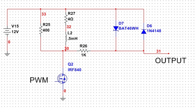
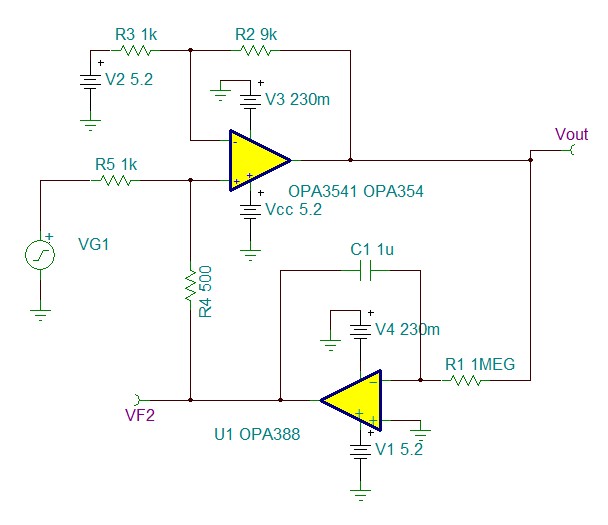
THIS SIGNAL COME FROM INDUCTIVE SENSOR.LEAST CHANGE IN SENSOR ENVIRONMENTS MAKE 20 MICRO VOLTS ON OUTPUT SENSOR.SENSOR OUTPUT SIGNAL CHANGE ALONG X AXIS AND EXPONENTIALLY CHANGED IN DIFFERENT CONSTANT TIME AND ALONG Y AXIS NOT CHANGE.
I WANT DIGITIZE THIS SIGNAL WITH 0V TO 5V ADC INPUT RANGE WITHOUT USE CAPACITOR FOR FILTER AND REMOVE DC OFFSET.
I PUT TWO PICTURE FROM SIMULATOR
AND OTHER
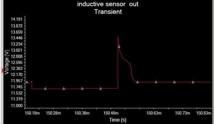
THESE PICTURES SHOW OUTPUT SENSOR CHANGES .
EVERYONE CAN HELP ME FOR AMPLIFY AND CONDITIONING THIS SIGNAL??
THANKS
SINCERELY.
Hi Reza,
Here is a concept that might work for you:
Inductive sensor OPA354 + OPA388.TSC
I'm not sure how sharp of an edge you have to your sensor signal or how narrow the pulse is so it's hard to say exactly how much bandwidth you need, but I think something like this will accomplish what you are after with some tweaking for your signal. The OPA388 is configured as an integrator that integrates the output and feeds it back to the input of the OPA354. Note the phase inversion effectively makes this negative feedback. This strips off the dc offset without loading your sensor. There will be a long startup time associated with this depending on where you choose the cutoff frequency with R1 and C1. You want the response time to be relatively slow so that you filter out the dc and don't distort your sensor signal. You will likely need to adjust things to get the optimum response for your sensor.
Thanks for reply.
In my circuit maximum rise time is 70 Nano seconds.
I complete your circuit and resend two schemes for you. please verify these .
In scheme 1.tsc I add sensor and change R1 and C1(integrator) because circuit respond is slow and when signal fall ,pass lower from base line.
In scheme 2-sw.tsc I SHIFT 200uS VG1 and add a switch for sampling base line of signal.(we can add any SPST).you can simulate.
I send two schematics for you, please verify and give your VIEWPOINT.
1-What scheme is best? (your scheme or scheme I send for you)!
2-how can divide exponential fall two segment and verify each segment?(I think when amplify this signal max 5v have not enough dynamic range).
3-if I change D1 ,D2 with BAT86 (OR LOW VOLTAGE SCHLOCKY_DIODE)can give best dynamic range.
THANKS
Sincerely.
Hey Reza,
Sorry for the delayed response. I like the idea of switching the integrator in and out to avoid issues with the input voltage shifting because of the transistor turning on and off. The dynamic range problem can be tricky to address. One way you could approach it is to have multiple stages: one stage that runs in a high gain meant for amplifying low signal levels, and another that feeds into a difference amplifier and subtracts a reference voltage from the signal before amplifying it again. See attached for rough example. If you scale things accordingly, then only one channel would have a valid signal while the rest would be saturated so you could use that to determine which range you are in and what the actual signal level is.
Hi
Thanks for replay
I am in a hurry! Sorry.
I did not understand your writing. Please explain again.(explain about switching and transistor)
This scheme I send for you detect ferromagnetic from paramagnetic metals.
If paramagnetic near to sensor the transition when fall reduced width, and if ferromagnetic near to sensor, more width of falling transition.
my questions are:
1-if replace D1 and D2 with Schottky diode, can get more dynamic ranges??(Because these diode turn on with lower voltage)
2-i sends a scheme for you. Please tell me what scheme is best?(this or your scheme)
Thanks for the answer sooner.
Sincerely.
Thanks for replay
1-DIODE D2, when used a diode with less forward voltage (Vf) and when switching transistor turn on, so having less voltage drop from other diode. This area have not information’s (Sensor voltage contain information on falling exponential segment you can see in TINA ) and we can more amplify signal for get more dynamic range and saturate op amp and remove other segments.
2-DIODE D2, clamp EMF high voltage when T1 turn off.my questions is: if uses lower Vf diode better or higher Vf diode??this diode turn on with lower voltage is best or turn on with higher voltage?
3-i wants digitizing falling exponential segment of signal not whole segments. (I use ADS8329 1MSPS and 16 bits) So need falling segment more amplify (when more amplify and op amp saturate so width of falling segment be more and on this state if sensor sensing Ferromagnetic, this width will be more and if paramagnetic Sensing , this width will be less, because my digitizer sampling each micro seconds I need more amplify this segment . please give best method.
Please write simple.
Thanks
Regards.
See attached for a recommended circuit that I think will be more applicable for what you are trying to achieve.