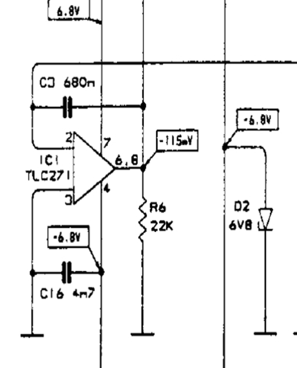
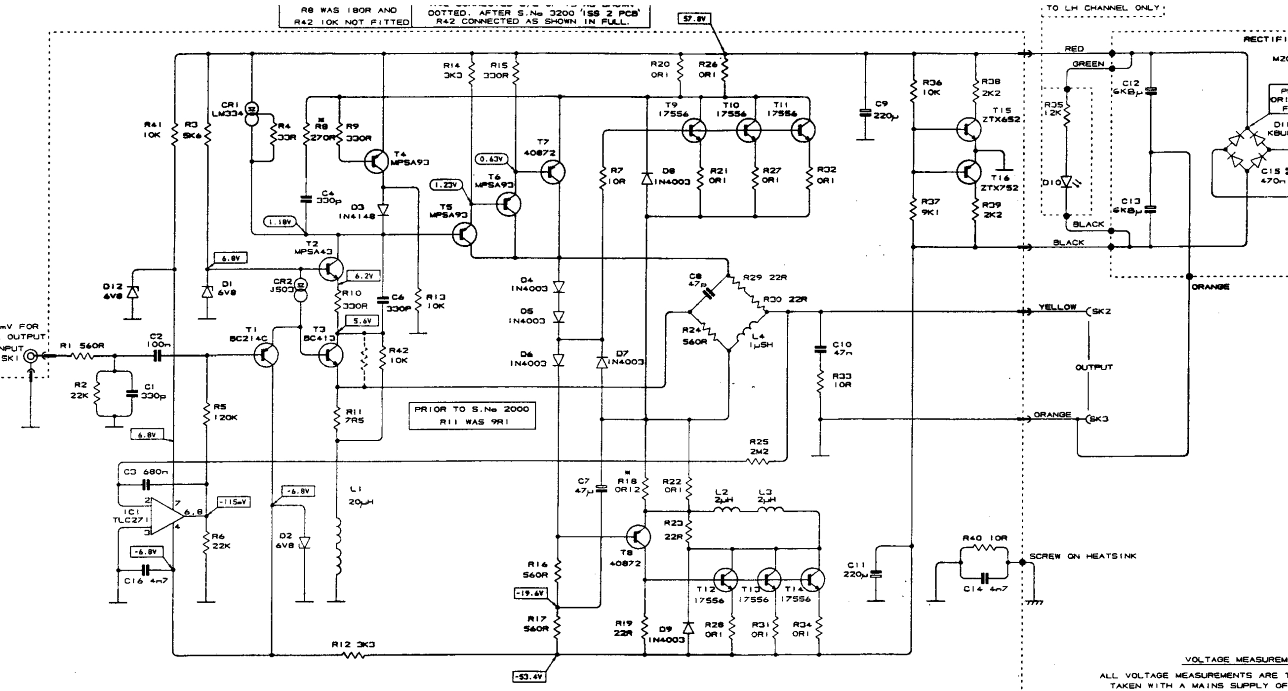
This thread has been locked.
If you have a related question, please click the "Ask a related question" button in the top right corner. The newly created question will be automatically linked to this question.
this IC's in this configuration- can it be programmed or is met to be just a drop in part that should work as is
if it can be programmed how do I do it ?
it works like it is but I am getting a little DCmv on the out put of the power amplifier it is adjusting for
OH there is a -6.8v on pin 4 and + 6.8v on pin 7 and 115mv on pin 6,8 there is a 2.2 meg on pin 2 going to speaker outputs
thanks
Hi Mike,
The TLC271 is advertised to have a programmable power consumption based on the setting of the "Bias Select" pin (pin 6).
It sounds you're asking if there's a way to program the input offset voltage so you can trim the output voltage to 0V. The TLC271 and most modern op amps without trim pins do not have a way to program the input offset voltage to a particular level other than using an external trim voltage which depending on it's accuracy may be better or worse than the TLC271 is already providing.
Without seeing the full circuit configuration it's hard to debug if there may be an issue but a first recommendation would be to migrate to a newer device such as the OPA170 which has better input offset voltage and input offset voltage drift specifications.
thanks Collin first this is the older plug in IC style type in use also i have seen other schematics pin 3 is open and pin 1 is grounded
I was just wondering if it holds a program if momentarily touching a pin ether grounding or a voltage with out adding external parts ?
of coarse if I could add a control to get 0v dc in the output ckt that would be great.
this problem I am having may be from other parts of the ckt that drifts over time it is just that it happened after changing the IC
I guess I am suppose to get a stable 115mv on pins 6&8 for it to work right? or what would most likely give me ov DC on the speaker out
thanks Mike
Hi Mike,
the TLC271 is working like a DC servo here. As the circuit looks a bit old I guess that in an earlier version another OPAmp was used, an OPAmp with a different pinning.
The DC servo works as follows:
Pin 3 of TLC271 is at GND potential. By the help of negative feedback pin 2 is held on virtual GND. When the output of power amplifier shows a potential which differs from GND, a current is flowing through R25 and C3 is charged. This circuit is just an integrator. As consequence the output voltage of TLC271 rises and shifts the operating point of input stage of power amplifier, T1, until the output voltage of power amplifier also shows GND potential.
So, the output voltage of TLC271 has not to be trimmed to -115mV, but is tuned to this voltage automatically when the DC servo loop stabilizes and the regulation of output voltage comes to rest.
The only error the TLC271 introduces is its own input offset voltage, which is 12mV worst case. I don't think, that this rather low input offset voltage must be trimmed to zero?
Pin 8 is the bias select input of TLC271. This is no output! To which potential is pin 8 connected? Can you tell us?
Kai
T1 e= -.64 b= .04 c= -6.7
T2) e=6.03v b=6.6v c= -56v
T3 c= 5.3v b= .64v e=.015v
T6 e= -.62v b= -1.2v c-56v or 1.6v from Ground
T5 b=-1.7v e=1.23v
r16=-28v other side r16 D6= -.6v
IC1 pin 6= -.033 pin2 & 3 are 0v pin 7=6.7v pin 4= -6.7
T15 B.=5v e= 0v c= +64v
T16 B=.5v e=0v C= -52v
R 39 1 side -52v & -59v -- looks a little burnt)
R38 1 side +64v & + 64v looks ok
I switched the card to the other side with the good caps and D11 It does the same thing and left on long enough
the B+ goes past 65v up to 77v while the other side goes down to 50v what else could cause this big imbalance ?
yes on both cards even C7
UP date I had a bad conection on R39 & t6 causing the offset
also R5 on the schematic shows 120k but some one did a mod & used a 62k resistor
I tested a 100k the voltage went up to -77 mv on pin 6 so if i go up 20k more that might put me at the -115mv Is there anything wrong with the mod being at 30mv on pin 6
if it is not hurting anything I could leave the 62k in there what do you think?
I have only 1 more problem one side is good at 1mv dc on the output the other is at 17mv and is slower
getting to that voltage I thank you very much for the help also i does chip regulate this DC bias ?
the voltage at pin 2 was 0v .
I don't know what happen after checking all parts again all were good
so I cleaned the boards with brake cleaner dried them and re installed
now both boards work and I get 0v DC off set on both outputs they works great!
I thank you very much for your help.