This thread has been locked.

If you have a related question, please click the "Ask a related question" button in the top right corner. The newly created question will be automatically linked to this question.

LMP91000: Vout is not as expected

Genius 5355 points
Part Number: LMP91000

Hi Support,

Customer has a problem in that the output voltage has no changes according to the BIAS register they have set.  I2C function OK.

The procedure of testing as follow:

  1. I2C checking LMP91000 available to communicate. (I2C address 0x00)
  2. I2C configured LMP91000 setting and turn IC.
  • I2C address 0x01 - unlock setting register
  • I2C address 0x10 - set TIACN
  • I2C address 0x11 - set REFCN
  • I2C address 0x12 - set MODECN


Tried settings:

TIA_GAIN       = 2.75KOhm, 3.5KOhm, 7KOhm, 14KOhm, 35KOhm, 120KOhm, 350KOhm.

RLOAD            = 10Ohm, 33Ohm, 50Ohm, 100Ohm.

REF_SOURCE = External, we are using external Vref as an input

INT_Z              = 20%, 50%, 67%

BIAS_SIGN & BIAS will change accordingly to our desire voltage.


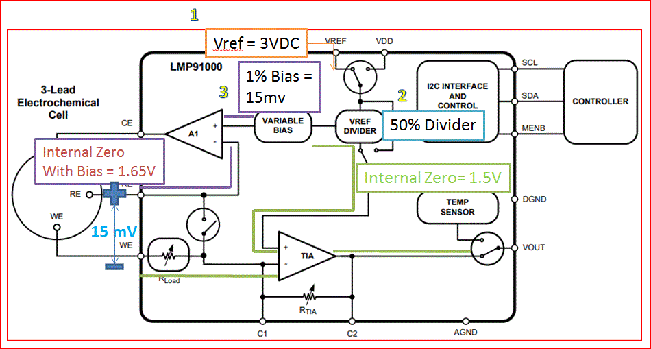
According to Dr. formula (LMP setting excel sheet), we are expected to get 15mV from LMP91000 Vout when Vref is 1.5V and BIAS configured to 1%. Unfortunately, the result after testing is far from the expected value.

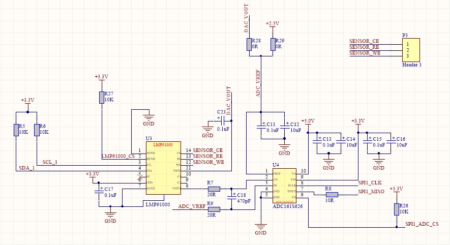
Attached the schematic and settings files.

Thanks.


LMP setting.xlsx

  • Hi Ikon,

    Applying a 1% bias to a Vref of 1.5V will apply a 15mV bias voltage to the sensor between the WE and RE terminal. If the sensor requires a 15 mV bias, then this setting is correct.

    From the datasheet of the sensor, do you know what load and bias are required for the sensor to operate? Could you share what kind of sensor this is?

    Could you please provide the settings that you used, and an output value that result from those settings? For example, when you set TIA_GAIN = 350K and R_Load = 10 ohms etc..., vout is 50 mV.

    I would highly suggest that you take a look at the webbench design tool for the LMP91000, located on the right hand side of the website

    This tool will help to find values required for your expected output.

    Best Regards,

    Dan

  • Hi Dan,

    Customer cannot set the voltage between CE and RE, their target is to get between 0 to 1 volt.

    Customer is using voltage base sensor.

    Thanks.

  • Hi Dan,
    In addition, the highest output I get from testing is about 10mV with TIAGN set default 2.75K, Rload 100R.
    As I understanding from datasheet, the bias voltage setting seem doesn't take 100% input from Vref. Accordingly to the block diagram, in the middle of input to output is having a voltage divider, what is the divider function as?
    Thanks.
  • Hi Ikon,

    The sensor should have a datasheet that will give the required values for bias voltage and the ohmic load required. These are required to ensure proper sensor operation. Is this a two lead or three lead sensor?

    Did you mean they want 0 to 1V between RE and WE (this is the sensor bias voltage)? When the sensor detects its target gas, CE will sink/source current through WE and the TIA (providing a voltage out). RE provides the reference voltage and will not sink/source any current.

    I have found that this app note is helpful in explaining the full functionality of the potentiostat in regard to gas sensors.

    The voltage divider, seen in the below picture, will provide a fixed offset voltage to the TIA.

    This is used to help maximize the response of the LMP91000 with respect to the ADC that will be reading VOUT (example 0.6V to 1.26V ADC sampling window). This can be controlled by setting the INT_Z register. You should see a direct change in output voltage (VOUT) when changing this value.

    Hope that helps.

    Best Regards,

    Dan

  • Hi Dan,

    Thank you very much for your reply. Actually the sensor that customer is going to use is a 3-lead electro-chemical sensor. They want to read the sensor data using a pulse voltametry technique in which the step voltages are applied to the sensor and its current is read. The voltages applied to the sensor are varied from 0 to 1 V with a 15mV step increment (please refer to the attached image for the voltage waveform applied to the sensor. 

    To do so, they have designed a circuit (as shown in the attachment) in which the Vref of LMP is sourced from a DAC. With the combination of DAC output and LMP voltage divider circuit we are creating the desired voltages for the sensor.

    Before they connect the sensor to LMP, they wanted to make sure that the circuit is able to produce the desired voltages between WE and RE. For this purpose, they have connected two 300 ohm resistors; one between WE/RE and one between CE/RE. However, they were not able to produce the voltages wanted.

    For example, to apply a 100mV voltage to the sensor, they used a 5V reference voltage and the bias setting of (2% of Vref). However, the voltage read at WE is only 10mV.

    Question: Understanding about LMP operation is correct? in other words, is it possible to create various voltages at WE with the combination of Vref and bias setting?" 


    Thanks.

  • Hi Ikon,

    Thanks for this thorough explanation.

    One issue I can see causing a problem is the internal zero setting (INT_Z). When I explained that the vref divider is providing a bias voltage for VOUT, I failed to mention that this voltage is also felt at the WE terminal (internal zero).

    Example (Picture below): If you have a Vref of 3V, the default Internal Zero is 50% (INT_Z = 0x01) , so 1.5V will be felt at RE, WE and at the output (VOUT). The Bias voltage (if used) will take a percentage (lets say 1%) of the Internal Zero so now there will be 15 mV bias (1.5V*1%) between RE and WE.

    My suggestion is to set the Internal Zero to 0% (ground reference, 0x11) in order to get 0V starting point. From there, you can use the bias and Vref of your choice, and should see the values you had previously calculated. Please note that this may not be desirable for your VOUT dynamic range.

    Hope that helps.

    Best Regards,

    Dan

  • Hi Dan,

    Thank you very much for sending the additional info and the diagram.

    Just for clarification, would you please confirm that the WE & RE voltages are calculated as below?

    - WE voltage is equal to Internal Zero which is the output of Vref Divider : (V_WE = y * Vref; in which y=20%, 50%, 67%,100%)

    - RE voltage is equal to [V_RE = (1+x) * V_WE] in which x= 0%, +1%,+2%, ...+24%

    Thanks.

  • Hi Dan,

    After I have done several testing with different setting, I couldn't get the expected figure.


    Vref = 2.7V

    RE is probed to positive terminal voltmeter.

    WE is probed to Negative terminal voltmeter.


    According to your explanation, Vref = 2.7V, INT_Z = 50%, BIAS = 1% and the output from RE to WE will expected to get 13.5mV. Unfortunately, I only get 0.3mV. 


    The following is the LMP91000 setting and output:


    TIACN(0x10) - 0b00000111

    TIA_GAIN = 2.7K

    RLOAD    = 100R


    MODECN(0x12) - 0b00000011

    FET_SHORT = DISABLE

    OP_MODE   = 3-lead amperometric cell


    REFCN(0x11) - 0b10010001

    INT_Z = 20%

    1% BIAS

    WE,RE = 0V

    REFCN(0x11) - 0b10010010

    INT_Z = 20%

    2% BIAS

    WE,RE = 0V

    REFCN(0x11) - 0b10010011

    INT_Z = 20%

    4% BIAS

    WE,RE = 0V

    REFCN(0x11) - 0b10010100

    INT_Z = 20%

    6% BIAS

    WE,RE = 0V   


    TIACN(0x10) - 0b00000111

    TIA_GAIN = 2.7K

    RLOAD    = 100R


    MODECN(0x12) - 0b00000011

    FET_SHORT = DISABLE

    OP_MODE   = 3-lead amperometric cell


    REFCN(0x11) - 0b10110001

    INT_Z = 50%

    1% BIAS

    WE,RE = 0.3mV

    REFCN(0x11) - 0b10110010

    INT_Z = 50%

    2% BIAS

    WE,RE = 0.3mV

    REFCN(0x11) - 0b10110011

    INT_Z = 50%

    4% BIAS

    WE,RE = 0.3mV

    REFCN(0x11) - 0b10110100

    INT_Z = 50%

    6% BIAS

    WE,RE = 0.3mV  


    MODECN(0x12) - 0b00000011

    FET_SHORT = DISABLE

    OP_MODE   = 3-lead amperometric cell


    REFCN(0x11) - 0b11010001

    INT_Z = 67%

    1% BIAS

    WE,RE = 0.6mV

    REFCN(0x11) - 0b11010010

    INT_Z = 67%

    2% BIAS

    WE,RE = 0.6mV

    REFCN(0x11) - 0b11010011

    INT_Z = 67%

    4% BIAS

    WE,RE = 0.6mV

    REFCN(0x11) - 0b11010100

    INT_Z = 67%

    6% BIAS

    WE,RE = 0.6mV  


    MODECN(0x12) - 0b00000011

    FET_SHORT = DISABLE

    OP_MODE   = 3-lead amperometric cell


    REFCN(0x11) - 0b11110001

    INT_Z = Internal zero circuitry bypassed (only in O2 ground referred measurement)

    1% BIAS

    WE,RE = 0.9mV

    REFCN(0x11) - 0b11110010

    INT_Z = Internal zero circuitry bypassed (only in O2 ground referred measurement)

    2% BIAS

    WE,RE = 0.9mV

    REFCN(0x11) - 0b11110011

    INT_Z = Internal zero circuitry bypassed (only in O2 ground referred measurement)

    4% BIAS

    WE,RE = 0.9mV

    REFCN(0x11) - 0b11110100

    INT_Z = Internal zero circuitry bypassed (only in O2 ground referred measurement)

    6% BIAS

    WE,RE = 0.9mV  


    Is there any load need to be added before probe to the RE, WE?

    Thanks.


  • Hi Ikon,

    Was the sensor connected when taking these measurements? Have you verified that the internal zero voltage is present (Measuring RE or WE with respect to ground)?

    When a bias voltage is present in your measurements, the bias voltage is not changing with respect to a change in the bias settings. I am looking into this further.

    What is the impedance of your probe that you are measuring with?

    Best Regards,

    Dan