This thread has been locked.

If you have a related question, please click the "Ask a related question" button in the top right corner. The newly created question will be automatically linked to this question.

TLV316: RRIO AOP how to minimize the output load effect

Part Number: TLV316

Hi E2E team,

I use a TLV316 as a follower for the output stage of my sensor.

The sensor output can be analog 0-5V or PWM 0-5V 500Hz.

The ouput load (after the TLV316) can be a pull-up or un pull-down between 2k and 100k ohms.

In factory, the sensor is calibrated without load. When the device is installed in the final equipment, the calibration must  not derive from these limits :

 - VIN=0.5 or 4.5V - deltaV max = +/- 25mV

 - VIN=2.5V - deltaV max = +/- 18mV

TLV316 is powered in 0-5V.

For now, I'm getting these results:

These values are the result of : (Vout with Pu or Pd) - (Vout with no load)

Pu 2k Pd 2k Pu 4k7 Pd 4k7 Pu 10k Pd 10k Pu 47k Pd 47k Pu 100k Pd 100k
diff / noPull diff / noPull diff / noPull diff / noPull diff / noPull diff / noPull diff / noPull diff / noPull diff / noPull diff / noPull
4,5V 0,009 -0,064 0,004 -0,027 0,003 -0,014 0,002 -0,002 0,002 0,000
2,5V 0,038 -0,034 0,008 -0,005 0,009 -0,006 0,002 -0,001 0,002 0,002
0,5V 0,064 -0,009 0,028 -0,001 0,013 -0,002 0,001 -0,002 0,000 -0,001

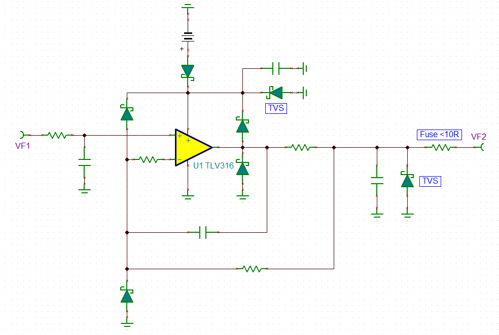
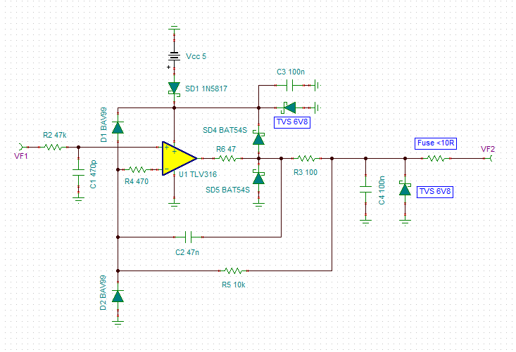
with this schematic :

Can you propose me a solution which can be compliant with my requirements ?

Thank you for your help,

Best regards,

Bertrand.

  • There was a problem with the schematic :

    TLV316 schematic.pdf

  • Hi,

    I guess this has to do with the finite resistance of the fuse? In combination with the pull-up or pull-down resistor a voltage divider is created. This can result in a big output offset voltage then.

    But there are some more issues:

    C203 should not be connected between the input pins of TLV316. This can erode the phase margin and cause oscillation. Connect this cap from the +input to signal ground.

    C205 directly at the output of TLV316 can also erode the phase margin and cause stability issues. Section 8.3.5 of datasheet of TLV316 shows how to handle big output capacitances.

    By the way, what is the purpose of the fuse? Which component do you want to protect by it?

    Kai

  • Is the above data provided when the sensor is in analog output mode or in PWM output mode?

    -Paul
  • Kai : The fuse is used to protect TLV316. Fuse F2 and the diode D200 protect the TLV316.
    I have a requirement from my client that is: the equipment can withstand a voltage of 18V on the output due to a wiring error
    I'm OK to connect C203=470pF between V+ and GND. C205 is already unconnected.

    Paul : The above data provided are obtain with the sensor in analog output mode.
    It's also true in PWM mode but it's not a problem. The information is in the duty cycle and the signal must between 0.5 and 4.5V.
  • The fuse is used to protect TLV316. Fuse F2 and the diode D200 protect the TLV316.
    I have a requirement from my client that is: the equipment can withstand a voltage of 18V on the output due to a wiring error
    I'm OK to connect C203=470pF between V+ and GND. C205 is already unconnected.

    Bertrand.
  • Hi Bertrand,

    allthough the BAT54 is a Schottky diode its voltage drop will be very high, if the current is not limited. Also, shunting the overvoltage current to the supply rail might not solve the problem, if the supply voltage cannot absorb this current. I think you need additional protection measures.

    Kai

  • Hi Bertrand,

    I would do it this way:

    Kai

  • Hi Kai,

    Thank you for this schematic.

    Last week, I done EMC tests. I think that the EMC configuration causes stability issues and I see an emission at ~190kHz.

    I have also some issues in susceptibility so I think the output capacitor is needed.

    We must take in consideration the requirement which is to have no deviation if I connect a pull-up or down of 2k ohms (0.18mV max). To be compliant, the R serie most not be greater than 11ohms.

    The fuse impedance is arround 10 ohms so it's not possible to add R serie and your proposition of schema can't matche with all my requirements.

    So, do you have another technic which can be compliant with :

    - an analog signal (f=0MHz) and a PWM signal f=500Hz

    - to have no deviation with a pull-up or down of 2k ohms (0.18mV max).

    - be as cheapest as possible

    Thank you for your help,

    Best regards,

    Bertrand.

  • Hi Bertrand,

    the additional protection resistor located directly at the output of TLV316 sits inside the feedback loop. So, there will not be seen any voltage drop by the load.

    Take care, the resistance of your fuse can widely vary. These polyswitches can have huge tolerances.

    Kai
  • Hi Kai,
    Thank you for your fast feedback.
    Do you have any recommended values for your schematic proposal ?
    Bertrand.
  • Hi Bertrand,

    this circuit could be a starting point:

    Eventually, the supply voltage should be increased a bit. Or you might omit SD1.

    Kai

  • Hi Kai,

    Thank you for these precisions.

    This solved my issue.

    Thank you for your quality support,

    Best Regards,

    Bertrand.

  • That's good news! :-)

    Kai