This thread has been locked.

If you have a related question, please click the "Ask a related question" button in the top right corner. The newly created question will be automatically linked to this question.

INA213: Random Component Failures

Part Number: INA213
Other Parts Discussed in Thread: SM72295,

We are experiencing random component failures / burn up of this part in a new product design which has been extensively reviewed by TI in the past.

We are not exceeding any of it's operating specifications and the components are properly oriented on the board

At this point, I believe that we may be receiving faulty components from either TI, the vendor or the assembly house.

We need to resolve this issue ASAP as we have just order 100 assemblies that use 3 of these components each.

Thank You in advance

  • Hi Nicholas,

    you might want to have a look at this thread:

    e2e.ti.com/.../637442

    Kai
  • mppt.pdfThanks for the response, Kai

    I will verify the version of the part I am using. I did not include the circuitry for transient protection however, the devices are used in an MPPT solar charger design that was derived from the TI SM72295 device eval board. (We are using the SM72295 device and are using the INA213 to monitor solar array and battery current instead of the those in the 72295 part) I can virtually guarantee that we are not having a problem with transients affecting the part. In addition to parts latching up, we have a few that are actually burning up i.e. smoke and fire, as if we were severely exceeding their operating limits... except that we aren't.  It is interesting to note the following... the INA213 that is used to monitor solar array current can see voltages up to about 21v on its inputs which is getting up to it's maximum limit of 26v while another INA213 is used to monitor battery charge current and may see voltages up to 15v. The part exposed to the higher voltage is the one that is most likely to burn up while the one used to monitor battery voltage is more like to latch up with a fixed output voltage without burning up. The ones that simply fail in latchup do get very warm however while powered in that failure mode.

    Let me know if you would like to see a schematic. I tried to attach one here.

  • BTW, how can I determine the version of the part? I will try answering this one on my own before I hear from you.

    Thanks Again
  • According to the package label, the date code of the parts we assembled is 1731. Other than that, I don't see a way to determine the version.
  • Hello Nicholas,

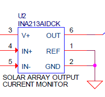
    Sorry to hear your team is running into issues with our INA213 devices.  I agree with Kai that the device ESD structure suffering latch-up could be the cause.  From the schematic you posted (figure below), the devices used appear to be the A version.  You should first replace those with either a INA213BIDCK or a INA213CIDCK.  Once you do that, please let us know if you still run into issues and we will try to see if they are other contributing factors leading to your device failures.


  • Hey Nicholas,

    In addition to ensuring that latch-up is not due to transients in system operation I would also check the difference between any ground planes. I am unaware of how your hardware is assembled, but according to the schematic there are two different ground symbols. One sysmbol for the INA213 and temp sensor and then another ground symbol for everything else. Are you sure there is a low-resistance connection between these two ground nodes? If not, there could be a potential voltage difference between them that slowly increases. This would effectively raise the common-mode voltage of the INA213 and easily destroy the device. I would recommend powering up a system with a voltmeter measuring the potential between both ground plans or two voltmeters measuring each ground plane with respect to Earth ground.

    Peter Iliya
    Current Sensing Applications
  • Hi Peter:

    The IAN213s are on a ground with most of the other circuitry except for that associated with the charging circuit i.e. on the MOSFET side of the SM72295. The 2 grounds are tied together through a large 0.0005 ohm resistor (R70) near the power supplies (Page 2 of the schematic) I forgot to mention that when these parts fail, they fail within 5 seconds after power up. By "Power Up", I mean connecting a live solar array to J1 and a lead acid battery to J2. If they don't fail within that time, they appear to work and continue to work quite well. We have 20 prototypes on hand now, 5 of which are still working after 1 day of operation and 2 which have been working for weeks now (including one in my office where I can monitor the behavior.)

    I suppose that we could be introducing a transient when connecting either one of those supplies however, solar arrays and batteries generally don't generate transients unless something else may be happening while making the connection. I will look at this with a scope. The TVS diodes and the MOVs we have across those connectors are usually quite effective at clamping any transients we've encountered on previous designs.

    Thanks for clarifying how to identify the version. We absolutely want to use version B or C to avoid this problem.

    I will give you more information as I continue to investigate this.
  • BTW, what is the difference between the B and C versions? Also, as mentioned, we have a few boards that seem to be working well. Not quite sure why we haven't damaged those yet? (although I know that failure modes can be hard to predict)
  • Also, the 2 ground planes are within 10 mV of each other.

    Just to give you a general idea of the layout, the board is 4 layer, layer 2 is a split ground plane. The SM72295 is sitting roughly at the center of the board with the split running under it. The switching MOSFETS and other charger components are to the left of the split (Earth ground symbol) and the digital components are to the right of the split (signal ground symbol) Since the INA devices have their sense resistors in the charge path, those devices are located on the Earth ground side and have their grounds routed to them from the other side (Signal ground). I don't think that would hurt anything but just thought I'd run it by you.
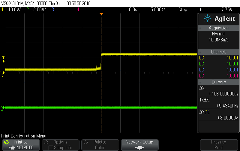
  • Here are some scope shots as I connect the battery (top shot) and the solar array (bottom) across their respective connectors. I don't see any evidence of spiking / transients / etc as I make the connections.
  • Hi Nicholas,

    please connect a protection TVS directly (!) from each input pin of INA213 to the GND pin of INA213, with as short as possible connection! Do this with each INA213!

    Kai
  • Hi Kai!

    I have been using a scope to look around a defective board vs a good board and have verified that I do not have any ground faults or transients that may be affecting these parts.


    That being said, I do have an idea that I want to run past you. Looking at the schematic, we use 3 INA devices, U2, U3 and U6.
    U2 and U3 power up from the 3.3v supply while simultaneously having 12v applied to their inputs. OTOH, U6 does not see input voltage until we drive Q1, long after Vdd has stabilized. So far, we have not seen any failures of U6. Is it possible that these parts cannot tolerate the race condition that may exist between Vdd and common mode input voltage?
  • Also, since we are using the DCK package, we can't experiment with connecting TVS diodes from pin to GND.
  • So, according to the datasheet...

    >>Note also that the INA21x can withstand the full input signal range up to 26 V at the input pins, regardless of whether the device has power applied or not.<<


    I suppose this answers my question above unless there is another factor at play.
  • Is this thread still being monitored???


    We were able to resurrect 4 boards on which U2 and / or U3 went defective by replacing them with version C parts (version B on one board). So far, there 4 boards are operating correctly and the parts have yet to fail as the version A parts did i.e. on power up. So far, I not noted any ground faults and no transients, let alone the 2 kV/uS transients that are called out in the datasheet. I also verified that the fastest input rise time that these parts see is about 3v /uS.

    So, although the datasheet states that these parts can withstand input voltages without being powered, I am leaning towards the version A parts having trouble with this.
  • Hi Nicholas,

    your boards carries lots of MOSFETs. These parts can switch very fast. In combination with the layout inductivities lots of transients and inductive kick backs can be produced.

    Following my recommendation of using TVS between the inputs and GND of each INA213 would at least answer the question whether such hidden transients are responsible for the latch-ups.

    Kai
  • Thanks, Kai!

    We will addthe transorbs and resistors to the INA inputs as recommended in the datasheet for transients above 26 V on the next rev of the board.

    We do get a good amount of switching noise coincident with the operation of the MOSFETS in the charge circuit which are driven by the SM72295. This noise, although difficult to measure, may be exceeding the 26v rating of the of the INA part.

    I want to point out the following however... the "general use scenario" is to first connect a power source to J2 (before connecting the solar array to J3). This source is typically the lead acid battery to be charged, which also powers the digital portions of the assembly. At this point, with no source connected to J3, the charging circuit is disabled and no MOSFETS are switching. Under these "quiet" conditions, we still manage to blow U2 and / or U3. This is why I believe that this problem may be related to power-up

    Again though, I do believe that we would benefit from adding the transient protection circuitry as you recommended.
  • Additional thoughts are greatly appreciated!
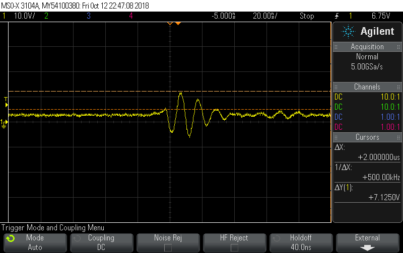
  • So far, the Version C parts are still working. I am still looking around with a scope however. The scope shot above is the 3.3v supply at the power supply pin and is a zoom in of the switching noise showing the voltage levels. How tolerant is the INA part to this? For comparison, there is almost no switching noise present at the inputs.

    Thanks for the help so far which will help us to address all of our issues on the next hardware rev.

    BTW, the rev C parts tend to be about 2% better on accuracy as compared tot he rev A parts. I suppose that this is due to improved gain error.
  • and sorry for posting so many questions... I'm also just trying to graduate from "Intellectual" to "Expert"
  • And, just to reiterate, there are no appreciable transients or switching noise occurring on the inputs of the INAs, at least during normal operation. Still going to add the tranzorbs and resistors on the next rev though that will help to avoid damage from transients from other sources.
  • Hi Nicholas,

    is the supply voltage of INA213 going negative? I don't think that this is good for the INA213...

    You could add some low pass filtering in the supply line. The use of a RC-filter could help.

    Kai
  • Hi Kai, yes, Vdd is swinging negative for the brief duration of the switching pulses whose frequency is 400 kHz. Although Im sure it's not causing the catastrophic failures were seeing with the version A parts, it certainly is far from ideal and could compromise the INA in the longer run. It is difficult to eliminate switching noise with these high - speed MOSFETS switching large amounts of current... perhaps RC filtering will help as you suggested.
  • Hello Nicholas,
    The difference between versions B and C is their ESD structures result in different gain error tolerances. As for why some of version A are still functioning can be attributed to device manufacturing variance making some devices more robust than others. All devices will have slightly different behavior, which is why we provide a typical value and then a minimum or maximum value for many specifications. Even with a max or min specified it is possible that 1 or 2 devices may operate beyond those limits. However all undamaged devices are guaranteed to operate within those limits. Unfortunately for the various versions of this device, we do not have a max input slew rate specified yet to avoid latch-up.

    As you ascertained from the datasheet, the common mode voltage and supply voltage requirements are independent of each other.

    If I interpreted your oscilloscope shot correctly, your supply is dipping well below ground from the switching noise. We do not have an absolute max spec for the lower limit listed, however, I will check with our design team and test engineers to see if I can get answer on what the impact of that operation is. In the mean time, an RC filter or simply a larger decoupling cap near the supply pin would be helpful

  • Very helpful information, thanks!

    As best as I can measure, the fastest slew rate that these devices see in this app is about 3v / uS while making the connections to the solar array and battery.

    I am starting to gain some confidence that the rev C parts can handle whatever it is that was blasting the rev A parts although the cause of that is still unclear to me. I am certain that it is not related to transients, switching noise or exceeding the operating limits. (I am still leaning towards a power up issue but we are not seeing any power supply surges, transients, or anything else unusual during power up) Again, when the rev A devices were failing, they were doing so within 5 seconds of being powered, while the charger circuits is not switching. Once past that point, good devices continue to work without failure.


    I will experiment with a larger decoupling cap on the supplies and will likely include RC filtering on the next board rev.
  • Hello Nicholas,

    I checked with our design team and the supply should not go lower than -0.3V with respect to ground. If it does, the device is expected to fail, yet the device failure may be gradual and exhibit a slow degradation in functionality.

  • Actually, some of that switching noise in the scope shot may be enhanced by probe ground capacitance... I'm trying to get a better measurement now...
  • So here is another scope shot using the tip & barrel approach across the bypass cap at the power pin. Note the V/div setting as compared to the last shot. Not nearly as bad...
  • Hello Nicholas,

    Glad to see that your supply pin is more stable than originally thought. As for your issue, we highly suspect that it was the startup conditions causing latch-up with the ESD structure found in version A of the INA213 device. Swapping out version A out with version B or C typically solves issues customers have with this device. However, during your ongoing tests, keep us posted on any new developments and we will continue to service you and solve this issue.
  • Thanks, Patrick, I agree that the problem is related to the version A device not tolerating our power up conditions. The version C parts have been working perfectly over the last few days. for now, we can call the issue resolved and I will post again if we run into any related problems.
    Thanks!
  • Hi Nicholas,

    for my personal taste the noise on the supply lines is a bit too high. If you plan doing a revision of your circuit, I would spend a bit input and output filtering on the switchers U13 and U14. Also, if not already carried out, each single chip should have it's own decoupling cap. Add a small resistance to provide an RC filter, if necessary. A few Ohms can help a lot!

    Eventually, the use of ground planes should be overthought. Usually, it is the best to have one solid ground plane, which is not splitted. The only reason to not allow certain ground currents to share the solid ground plane, is, if extremely high and spiky ground currents are flowing, which would totally erode the ground.

    Kai
  • Thanks Kai. We are changing the design to include low value resistors at the component pins in addition to the decoupling caps that are already there (might make those a larger value also) and to add filtering to the switching regulators. We are also eliminating the split ground plane which didn't help too much in isolating the digital ground from switching noise anyway.

    I have one update regarding version A component failure. I had mentioned above that we never saw U6 fail, only U2 and / or U3. We had a prototype unit running for about 1 month with version A components and U6 happened to fail just today. U7 and Q10 are used to switch the load off when the lead acid battery gets below 10.7v and switches the load on again when the battery gets back up to 12v. As it turns out, the prototype was being used in a unit that has a bad battery so the load was switching on and off at least once / day. I originally thought that perhaps the problem stemmed from a race condition between applying Vdd and a large common mode voltage (i.e 12v- 14v) but it now seems that just cycling the common mode voltage enough times (with Vdd constant) is enough to eventually cause the ESD structure to break down. So far, the version C parts are working well which is a good thing since we just shipped some units to a customer site.
  • Hey Nicholas,

    Glad to know the C parts are still working good for you. As for the late A failure, that is not unexpected. Failure resulting from ESD cells latching in A parts can be practically instantaneous or take several cycles before being noticed.

    As I said before, if you do run into further issues, please reply below. In the mean time though we will consider this thread closed.