This thread has been locked.
If you have a related question, please click the "Ask a related question" button in the top right corner. The newly created question will be automatically linked to this question.
Dear TI expert,
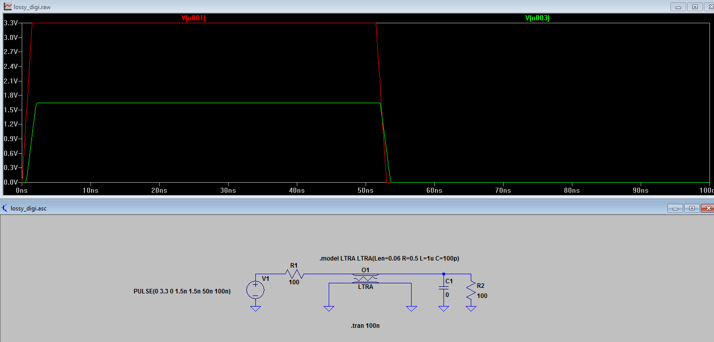
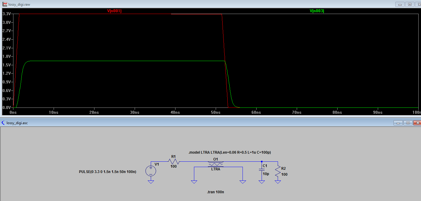
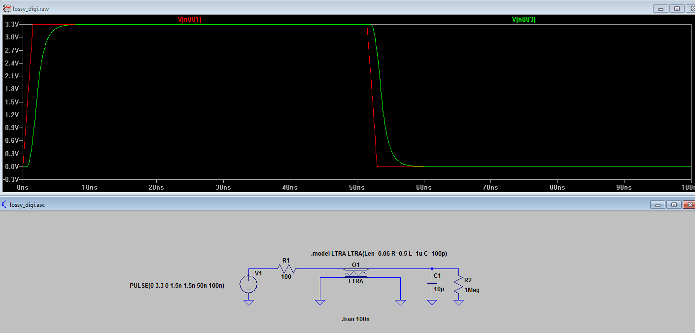
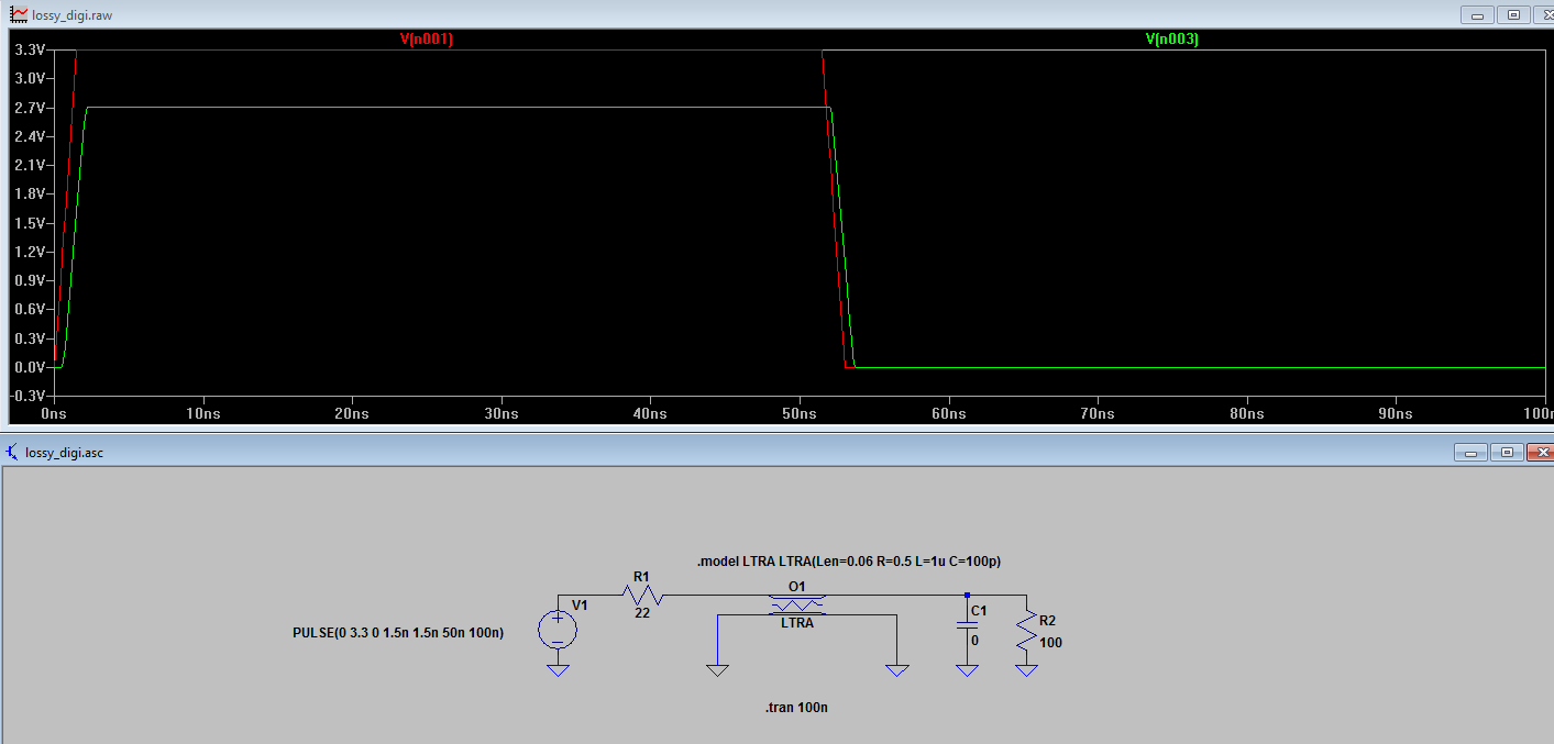
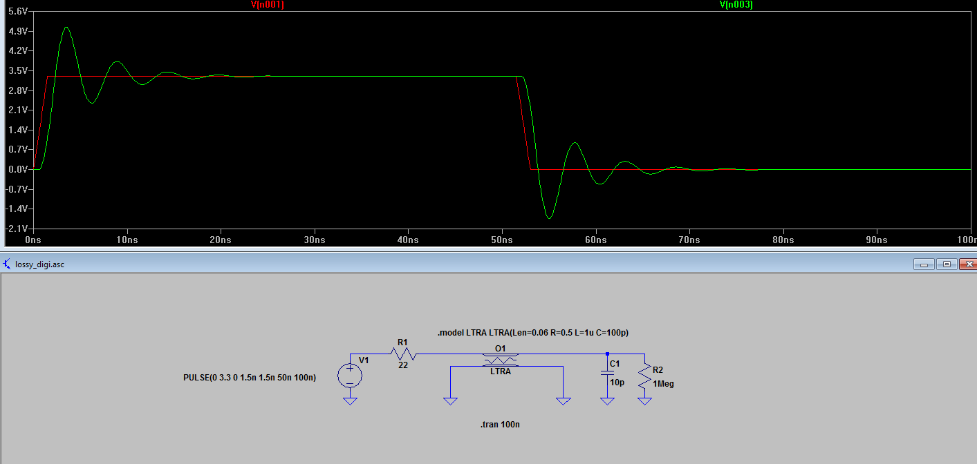
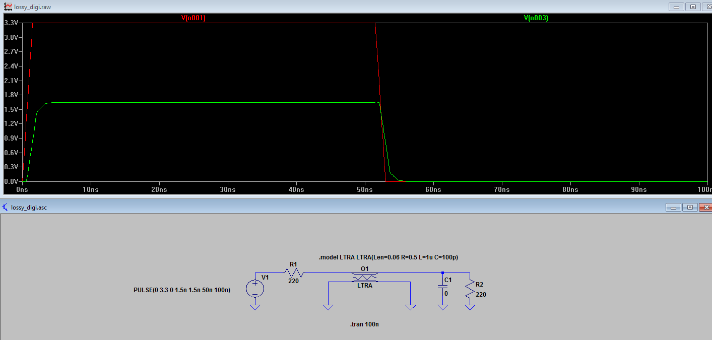
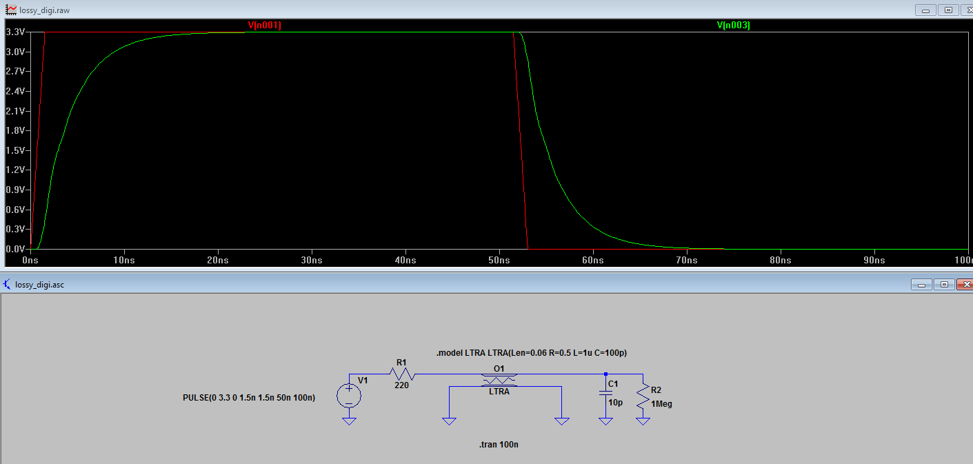
In my design, TLV3502's output is fed to FPGA. For the convenience, I want to design 2 PCBs and TLV3502 , FPGA are on seperate boards as Fig1. Both boards are connected by a pin-header.As you can see, on PCB1, TLV3502's output pin to pin-header is 25mm. The pin-header is 10mm and as Fig2. On PCB2, the pin-header is about 25mm to FPGA's realted pin. The traces on both PCBs are 10mil wide. TLV3502's operation frequency is low. I wonder with a ground plane below the whole trace,if this total 60mm distance too long for TLV3502 to work properly? Besides, should I use ground fills on the TLV3502-related traces' layers?
Fig1
Regards
Yatao
Hi Kai,
Thanks for your help.
Actually, the TLV3502 works at a period of no more than 10kHz and needs to toggle at 4 time points during each period. Take 10kHz as an example, as shown in Fig1, during each riod, it needs to work at 0.1us, 0.15us, 50us and 50.05us.
The reason why I must adopt high-speed comparators is because their delay is of critical importance for me. I need a comparator with as small a delay as possile.
Just to confirm, you mean it's ok for TLV3502 to go through 25mm long 10mil wide traces to a header-pin, who's 10mm long and then moves to another PCB to move another 25mm to FPGA?
Fig1
Regards
Yatao
Hello Yatao,
Yes. You should at minimum use controlled impedance lines, which at minimum is a specific width trace run over a ground plane. Google "Microstrip".
And as Kai said, when transitioning the connector, run a ground line on either side of the signal line - like the old IDE cables. 50 ohms is a heavy load. You may be able to go with 200 ohm trace and terminate with a 200 ohm resistor at the receiving end.
Can your FPGA accept LVDS inputs? You may wish to switch to the LMH7220, which is faster (3ns) and has a true differential LVDS output which will deliver a cleaner signal across distance. The LMH7220 datasheet also has a section on running the high speed PCB traces ("Microstrip"vs. "Stripline").
Hello Yatao,
The trace width on the PCB can be controlled during PCB layout. More advanced PCB fabricators will tweak the trace width to the required impedance values, but that is overkill for this application. You mainly want to reduce ringing and reflections that can distort the received waveform by trying to maintain a constant impedance (does not have to be perfect, ±20% variation is probably okay).
There will always be "discontinuities" when you transition over connectors, unless they were specifically designed for RF at a certain impedance. The best you can do is use a connector that has pin spacing close to the PCB trace to ground plane distance.
Have you thought of using tighter pitch or shorter connectors? 0.1" headers are from the 1970's 1MHz clock days.
https://www.digikey.com/en/resources/connectors/rectangular-connectors
The TLV3502 output has 1.5ns risetimes, so it should be treated as a 250MHz RF signal. The key thing to remember is that the ground currents will return directly under the signal trace, so the ground DIRECTLY under the trace should not be broken or diverted between the end points. The ground trace should be at least 3x the width of the signal trace.
So run the trace with the calculated trace-width, over an unbroken ground, and place a termination resistor at the receiving end equal to the trace impedance. You may wish to place a resistor directly in series at the output to allow tweaking of the end terminations for best waveform shape.
PCB stripline layout and header selection is beyond the scope of this forum - so we can't help much more here. But there are many PCB resources on the web, and many PCB layout tools will calculate the proper trace width when given the desired impedance, layer spacing and dielectric constant. Google "microstrip calculator" and you will find many. The dielectric constant of your PCB can be obtained from your PCB fab house (usually around 4 for generic FR-4).
Hi Yatao,
as so often in electronics it's not about making things perfect but to optimize the situation, to get the best of it with reasonable efforts.
So, in any case, use an isolation resistor directly at the output of TLV3502. Call this resistor series termination resistor, if you want. Even with an imperfect termination of characteristic impedances of traces and connector pins this isolation resistor will considerably help to dampen resonances and echos. I would use 51R as a starting point and increase it, if possible.
The next optimisation would be to embedd the signal trace in a ground plane within the same layer and to route the signal trace over a another ground plane. Try to provide a characteristic impedance of this microstrip line which is as high as the isolation resistor. Or by other words, try to route a 51R microstrip line, if the isolation (termination) resistor at the output of TLV3502 is 51R. Use the same microstrip line on the FPGA board.
With a bit luck you don't need a parallel termination resistor at the end of signal line close to the FPGA. This might only be needed in very demanding applications.
Of course, the connector will introduce an imbalance of characteristic impedance or discontinuity. But the connector pins are rather short and this might not have a relevant effect, especially if you use this isolation resistor recommend above. The higher this resistor the lower the ringing and echoing trouble, but the higher the unwanted comparator delay, too. Just check it out!
Kai
Hi Yatao,
yes, theory of characteristic impedance macthing says that the signal is exactly halved when using termination at both ends of the transmission line.
In the following you can see a simulation of the step response when driving a transmission line properly and improperly:
---------------------------------------------------------------------------------------------------------
-------------------------------------------------------------------------------------------------------
------------------------------------------------------------------------------------------------------
--------------------------------------------------------------------------------------------------------
------------------------------------------------------------------------------------------------------
--------------------------------------------------------------------------------------------------------
-------------------------------------------------------------------------------------------------------
-------------------------------------------------------------------------------------------------------
In all these simulations a transmission line of 100R and 60mm length is assumed. The source resistance of the voltage generator is zero and the rise and fall times are 1.5ns. (But keep in mind that the TLV3502 has a source resistance of about 50R.) The 10pF capacitance is the assumed input capacitance of FPGA.
Of course, these simulations are an idealization of what is actually going on in your circuit. But they show that R2 can be omitted, eventually. In any case make the series termination resistance (50R source resistance of TLV3502 plus R1) equal to the characteristic impedance of transmission line. When you increase the series termination resistance, the whole thing looks more like a low pass filter and when you decrease the series termination resistance, on the other hand, you will suffer from ringing. Ringing should be avoided, because it can turn-on the protection diodes at the input of FPGA and can cause lots of trouble.
Kai
Hi Kai,
You are so knowledgeable and warm-hearted! Thx again for sparing efforts to aid me. ^.^
I'm curious that, technically, are there questions regarding high-speed op amps and comparators that can stump u. ^.^
Regards
Yatao