Other Parts Discussed in Thread: THS4541, , ADS4245, VCA824, LMH5401, OPA859, ADS4225, THS3217, OPA656
Hi,
I am building a differential probe and a scope with ADS 4225. I am willing to have the LMH6518 inside the probe so that it is very close to the input buffers. My thoughts are that having the DVGA away from the buffers would introduce higher noise susceptibility due to the coaxial cable(s) connecting the buffers output to the DVGA. Now, if i do keep the DVGA close to the buffers (inside the probe), i would have to connect its' output to the THS4541 (ADC driver) input using 2 different coaxial cables so that i can keep the connection differential. However, i was thinking that after the DVGA, no significant gain would be necessary and thus using single ended connection would still be acceptable. In order to use single ended connection, i would have to use only one of the LMH6518's outputs, pass it through a 50Ω coax cable and terminate it with a 50Ω resistor right at the THS4541's input. 
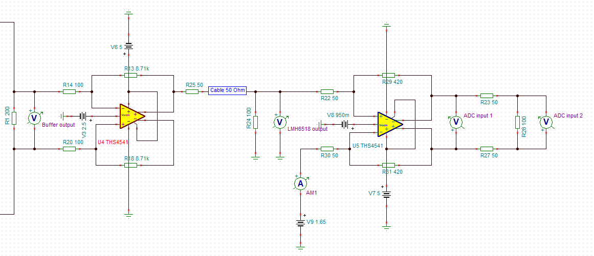
I have implemented a simulation circuit that has the buffers followed by a THS4541 (instead of the LMH6518) and then followed by the THS4541 (adc driver). (The LMH6518 TINA spice model is not available yet.)
The point where i have my doubts is the value of Rt which in conjunction with the Rg1+Rg2 must be 50Ω. The output CMV of the first THS4541 (replacement of the LMH6518) was set to 2.5V. However the voltage value at the point where Rt & Rg1 connect is now not 2.5V since the Rt form an attenuator with the 50Ω resistor internally in the LMH6518. Rg2 had off course to be biased to the same CMV that the Rg1 was so i used the 1.65V that you see to zero the output (diff) of the THS4541 on the right.
The snapshot of the TINA TI schematic works fine. I set the CMV of the THS4541 to 0.95V as the ADS4245 requires and i get the expected amplitude at the output.
Can you pls confirm if using such a connection between one of the LMH6518 outputs and one of the THS4541 is an acceptable way of connecting the two opamps?
I think there is something wrong in the Rt value. Its' value would be correct if the Rg2 was connected to GND but Rg2 is instead connected to 1.65V! Wha should i do there?
Any suggestions regarding the schematic?
Regards
Manos


