This thread has been locked.

If you have a related question, please click the "Ask a related question" button in the top right corner. The newly created question will be automatically linked to this question.

INA240-Q1: Setting the Reference Using a Resistor Divider

Part Number: INA240-Q1
Other Parts Discussed in Thread: INA240, INA282

Hi team,

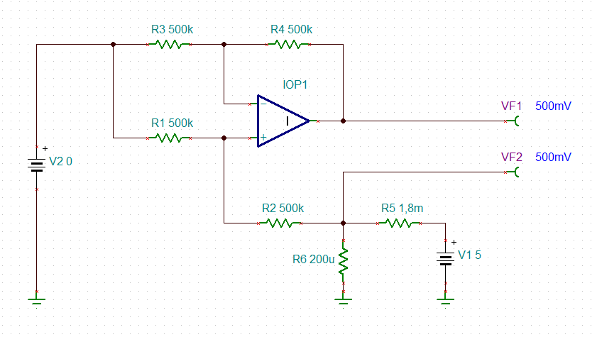
We are considering using INA240 as shown in the following figure.

Could you tell me the resistance value in red?

In our usage, current flows in from IN +, and the REF2 and REF1 voltages rise above the set value.

It is necessary to know how much the resistance value of R1 and R2 should be set.

Best regards,

Tomoaki Yoshida

  • Hi Tomoaki,

    you also might want to read this thread:

    e2e.ti.com/.../636656

    Kai
  • Hi Tomoaki Yoshida,

    Does the link provided answer your question? Please let us know if not.

    Thank you Kai for answering the question.

    Regards, Guang

  • Hi Guang-san,

    Thank you for your support.
    I understand the value of internal resistance.
    However, I do not understand about common mode error and differential output error of link destination.
    e2e.ti.com/.../636656

    The thread has the following expression:
    CMRR: R1/(2 * Rf) * 2.5V
    Gain Error: R1/(4 * Rf) * Vdiff * 20V

    There is 2.5 in the CMRR equation, which voltage is this?
    In the explanation, assuming 5V supply, we set external R1 and R2 to set the common mode voltage to 500mV.
    In our case, Should I substitute a design value of 500mV?

    I understood that the gain error formula 20 is the gain of that device.
    Is this also correct?

    Best regards,
    Tomoaki Yoshida
  • Hi Tomoaki,

    by introducing the voltage divider you degrade the symmetry of the differential amplifier within the INA240. The smaller the resistances of voltage divider the smaller the imbalance of differential amplifier and the less the degradation of common mode rejection.

    See the following simulations carried out with an ideal OPAmp. (Of course, the 1.8mOhm and 200µOhm resistances are idealized values only being used for clarity. They would never work in reality.)

    These simulations demonstrate the importance of what the datasheet recommends:

    "If the amplifier is used in this configuration, as shown in Figure 31, use the output as a differential signal with respect to the resistor divider voltage. Use of the amplifier output as a single-ended signal in this configuration is not recommended because the internal impedance shifts can adversely affect device performance specifications."

    You can take my simulation file to also estimate the gain error:

    tomoaki.TSC

    Kai

  • Hi Yoshida-san,

    The 2.5V common mode voltage comes from the fact that the output stage sees roughly 2.5V common mode (mid-scale) regardless of the input common mode voltage which can be anywhere in the -4 to 80V range. Therefore even if you use R1/R2 divider to set a reference of 0.5V, you should still keep the 2.5V in the calculation.

    Thank you Kai for the comments.

    Regards, Guang

  • Hi Guang-san,

    Thank you for your support.

    I understand.

    In another thread linked URL, it is pointed out that the resistance of Rf is trimmed for gain adjustment and has tolerant of +/- 20%.

    e2e.ti.com/.../559241

    How accurate is this 2.5V?

    Since we need to set the output common mode voltage to the set value of 0.5V + -10mV, we need information of 2.5V accuracy.

    Best regards,

    Tomoaki Yoshida

  • Hi kai-san,


    Thank you for the important information.
    I understood better.

    Best regards,
    Tomoaki Yoshida
  • Hi Yoshida-san,

    There is not a spec for the 2.5V common mode voltage, or mid-scale. It is set internally as common mode feedback for the fully differential portion of the amplifier. Its absolute accuracy is not critical for the operation of the amplifier, I would say it is probably safe to assume <5% base on common process technology statistics for resistors (ratio not absolute value).

    Regards, Guang

  • Hi Guang-san,

    Thank you for your support.

    I understand that the 2.5 V accuracy of the internal common mode voltage does not affect the output performance of the fully differential amplifier as you say.

    But, we want to receive the output with a single-ended ADC.

    This means that common mode errors appear as offsets in our system.

    If this requirement can not be met, then it is better to use a fully differential ADC, but we need to have a fully differential ADC and we don't want to do it if we can.

    In order to identify it, we need to accurately estimate common mode errors.

    Best regards,

    Tomoaki Yoshida

  • Hi Yoshida-san,

    Thank you for the explanation. I think you have all the information you need by now. But if not, please let us know.

    Regards, Guang

  • Hi Guang-san,

    Thank you for your support.

    I think we can calculate the common mode error by following formula.

     Common mode error = R1/(2 * Rf) * 2.5V

    Since R1 is an external resistor, the accuracy and resistance can be determined by the user.

    I recognize that 2.5V has the tolerant of +/- 5%, and Rf has the tolerant of +/- 20%. 

    The tolerance of Rf does not seem to be verified, but what is the maximum adjustment range?

    Or, please let me know if you have measured data or theoretical values.

    I would like to know if +/- 20% can be considered as worst.

    Best regards,

    Tomoaki Yoshida

  • Hello Tomoaki,

    Tomoaki Yoshida91 said:
    This means that common mode errors appear as offsets in our system.

    Perhaps ADC software (single ended) must subtract minor offset (500mV) to approximate a 0v current level?

    Tomoaki Yoshida91 said:
    In order to identify it, we need to accurately estimate common mode errors.

    Using a resistor divider to set REF output threshold <midVS may not benefit configurations where periodic common mode signals are monitored via low side Totem pole. Oddly the INA282 datasheet suggests precision error is expected the further REF deviates from mid VS, how did the INA240 correct this issue? Our test found +1.224v REF caused output to float above mid REF, during CM signal propagation (VS=3v3) any added output capacitance 1nF-22nF. The idle noise level is no less from mid REF, best noise level  20-130mV peak via 2mohm shunt no matter REF >GND. 

    Oddly Spice model 240 output with 10k pull down did not reveal mid REF error condition ever occurs.  

    Personally I would not use mid REF to monitor via single ended ADC and output resistor divider is not recommended for differential inputs. Best precision is achieve REF1,2=GND and single ended ADC may produce seemingly fair results for periodic (non-sinusoidal) CM signals. That may be due to external CADC charge share handling loop gain of certain SAR variety, you test! However it seems the differential amplifier CMRR/PSRR reacts to some CM transients in an odd way, that is more concerning in our issues!


  • Hi,

    Thank you for your reply.

    >Perhaps ADC software (single ended) must subtract minor offset (500mV) to approximate a 0v current level?
    Yes, since 500mV means 0A in our system, common mode error remains as an offset.
    That is because single-ended ADCs do not accept 0V input.

    Currently our concern is whether it is reasonable to estimate Rf at +/- 20% and 2.5V at +/- 5% for common mode errors.
    We think that it is sufficient for our judgment if there are actual measurement data that show the ability value, etc. Is there such data?

    Best regards,
    Tomoaki Yoshida
  • Tomoaki Yoshida91 said:
    That is because single-ended ADCs do not accept 0V input

    They do though the noise level (precision error) is often >1LSB settling time. Ideally we need SAR to settle 1/4LSB to achieve least possible error, no matter how REF is configured. Note we use 12bit single ended TI SAR and no added Cext, otherwise open loop gain (precision) between 240 output and SAR is effected in a bad way. So it seems 240 was not tested for TI SAR compatibility. Be aware there are other sources of error to contend with! 

  • Hi Yoshida-san,

    You’re doing the right thing to estimate the worst case error and see if it is acceptable. If it turns out to be too big, maybe we can consider a system calibration at zero current if possible.

    The INA240 can drive up to 1nF as is. If it is not enough, it can be increased up to 100nF while adding a 100Ohm isolation resistor.

    Regards, Guang

  • Hi Guang,

    Guang Zhou said:
    The INA240 can drive up to 1nF as is.

    Datasheet states 1nF loading without sustained oscillations, from the perspective of the applied circuit. That does not imply 240 has a maximum capacitive drive capability of only 1nF. The output short circuit graphs indicate much higher current drive is achieved irrespective of output (load) capacitance! The 240 output can drive >1nF loads, according to datasheet graphs no error in precision results. Reality being >1nF load, output transient response pulse/s are then elongated and sustained oscillations can easily occur in PWM pulse trains.

    If you consider sustained oscillations are indicative of precision or error, that seemingly has not been proven by datasheet graphs. It is only assumed by datasheet no capacitance was even added by laboratory testing to produce such pristine graphs. Better to no not add any filter on 240 output as it severally effects transient response (rise times) or SAR precision.  The other part being output linearity is effected or changes too >1nF.    

  • Hi BP101,

    When you say “The 240 output can drive >1nF loads, according to datasheet graphs no error in precision results”, which graphs are you referring to? And how did you draw the conclusion?

    Regarding definition of precision, the datasheet always quantifies it with a number, such as % or mV, uA and things in that nature. “sustained oscillation” is not such a quantifier, we never use it to indicate precision or error. In the datasheet’s context, the word is to indicate that there is no observable oscillation when driving 1nF.

    Regards, Guang